This thread has been locked.

If you have a related question, please click the "Ask a related question" button in the top right corner. The newly created question will be automatically linked to this question.

BQ76952: bq76952问题咨询

Part Number: BQ76952
Other Parts Discussed in Thread: BQ76942

bq76952问题咨询:

1 芯片规格书中看到此芯片应用范围包括无人机,为了防止无人机在飞行阶段触发保护后坠机,那么芯片内部的各种保护是否可以通过软件disable掉;
2 在无人机行业中使用,在飞行时,如果MCU异常或者复位,bq76952是否会受影响(比如:IIC通信超时;MCU复位后直接与芯片IIC通信是否可以成功建立通信;);
3 芯片适用于高边控制,官方也推荐了原理图,在原理图中Cp1引脚上的pump电容的容量是否与NMOs的并数相关联,如果有关联性是否有量化数据推荐(比如20并NMOS) ;
4 芯片改成低边控制,官方推荐采用DDSG与DCHG两引脚来做为控制NMOS的控制电压,这两个引脚除了电压与DSG和CHG不同外,控制速度和电流能力是否也不同,如果不同是否有相关数据提供进行参考;
5 芯片改成低边控制,官方推荐采用DDSG与DCHG两引脚来做为控制NMOS的控制电压,短路保护是否可以保证实施;
6 芯片改成低边控制,官方推荐采用DDSG与DCHG两引脚来做为控制NMOS的控制电压,是否可以继续用DSG来做放电MOS管控制,参考引脚PACK接B-这种方,充电mos用别的引脚来控制触决(比如PCHG);
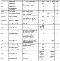
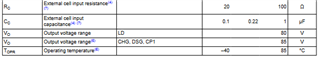
7 BQ76952的引脚等效图文档中,各个IO脚都有二极管,是否可以明确出耐压值;

  • 您好,正在询问更了解这款芯片的TI工程师,稍后回复。

  • 追问:

    8.bq76952芯片规格书中描述了静电防护值,如果实际在使用中静电超过规格书中的数值时,芯片会产生什么现象;

  • 您好,

    1. Yes, all protections can be disabled with the BQ76952 in Settings:Protection:Enabled Protections A,B, and C.

    2. The chip is designed to be able to function autonomously without an MCU, so an MCU going out wouldn't turn off the chip. However, if the MCU tried to reconfigure the BQ76952 on startup, the device does turn off the FETs when it gets reprogrammed. However, if the MCU doesn't do this on startup, resetting the MCU won't cause any issues.

    3. The general recommended range for the capacitor is between 470uF and 2uF for more FETs. I would recommended viewing this document, Multiple FETs with the BQ769x2 Battery Monitors for more information on parralelling FETs. In the document, they use both 470uF and 2uF for driving the gates. Both are operational at 24 FETs. The trade off between higher capacitance is that it will take longer to power up the charge pump, but it won't drain as quickly when first turning the FETs on.

    4. When using the DDSG and DCHG pins for low-side driving, there are two options: using them to drive the gates or using them as the control signal for a gate driver. Without the gate driver, the pins will be slower to turn off and on the FETs when compared to high-side since the two pins are more akin to digital signals. However, with a gate driver, the FETs will be turned off just as quickly (if not faster depending on the gate driver) then the DSG and CHG pins. However, another circuit would be needed to power the gate driver. Current capabilities are still the same.

    5. SCD can still be implemented with low-side control with the sense resistors being between BAT- and the FETs. I would reference the following reference design: TIDA-010216.

    6. The DSG pin can not be used to drive one of the FET gates when the device is configured for low-side switching. It produces a voltage 5.5V (or 11V) greater than the BAT pin, which means the Vgs of the FET in low-side would see upwards of 60-70V.

    7. For the withstandable voltages, I would recommend relying on the following table from the datasheet:

    8, 芯片会损坏或者进入保护.

  • 以上感谢回复。

    5. SCD can still be implemented with low-side control with the sense resistors being between BAT- and the FETs. I would reference the following reference design

    >>如果低边方案使用了门驱动芯片,驱动20并NMOS在电路中,为了保证SCD能完美保护,是否有特别注意点?

    另外,是否能够量化出DDSG与DSG之间的时间差?如果不能量化出来,是否能给出一个低边应用方案的DDSG短路保护时的接断时间波形?

    8, 芯片会损坏或者进入保护.

    >>这里如果静电损坏或者进入保护有评价方法界定出来原因吗?由其是进入保护现象。