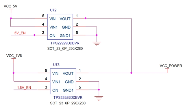
The following diagram is a schematic diagram of a dual power switch function that I designed using the TPS22929D chip. When the 5V-EN enable signal is high and the 1.8V-EN signal is low, VCP_POWER is 5V and 5V will not flow to VIN through the VOUT of U73;
When the 5V-EN enable signal is low and the 1.8V-EN signal is high, VCP_POWER is 1.8V, and 1.8V will not flow to VIN through the VOUT of U72;
May I ask if this design is acceptable? Hope to receive a quick response, thank you


