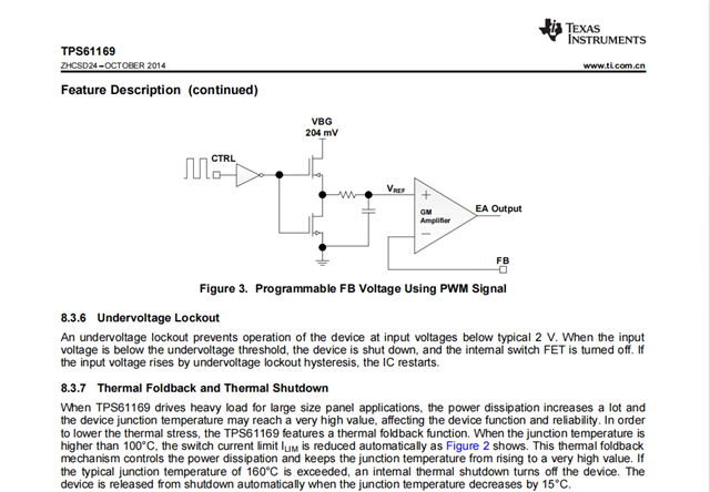
In the PWM control circuit for Vfb in the TPS61169 (image on page 10), why is the PMOS at the bottom and the NMOS at the top in the push-pull configuration, which is different from the typical push-pull driver circuits we usually see?

This thread has been locked.
If you have a related question, please click the "Ask a related question" button in the top right corner. The newly created question will be automatically linked to this question.
In the PWM control circuit for Vfb in the TPS61169 (image on page 10), why is the PMOS at the bottom and the NMOS at the top in the push-pull configuration, which is different from the typical push-pull driver circuits we usually see?
