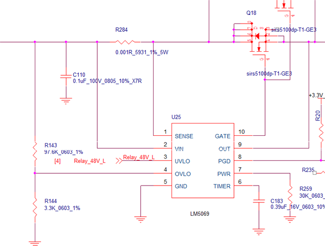
This thread has been locked.

If you have a related question, please click the "Ask a related question" button in the top right corner. The newly created question will be automatically linked to this question.

LM5069: Questions about the use of the chip

Part Number: LM5069

I would like to ask you some questions about LM5069,

1.If the LM5069 power supply and ground connection are reversed, will the chip be damaged?

2.As for the power limiting function, the VSNS voltage of the chip is recommended to be no less than 5mV (the sampling resistance is selected at 1mΩ, the maximum output current is 55A, so the minimum current is 5A when starting the MOS power limiting function). Since our input voltage is up to 60V, if the current is 5A, it is not less than 5mV. The maximum power received by mos will reach 60X5=300W, the stress on MOS is still too large, so a smaller current is needed to pass through MOS at this time, can I use a smaller VSNS voltage value? According to the specification, when VSNS is less than 5mV, the current sampling accuracy is not high, is there a more definite value for this accuracy?

3.After the chip is started, the maximum current set by our chip is 55A. Can the chip work normally when the load current is less than 55A (such as 45A)?

  • 您好

    针对您关于LM5069的问题,请参考以下说明:

    1. LM5069电源与地线接反的话,芯片会损坏吗?

    LM5069芯片在电源与地线接反的情况下,其损坏的可能性是存在的。然而,具体的损坏情况可能取决于电路设计、保护措施以及接反时的具体条件。一般来说,如果电路中没有适当的保护机制(如防反接二极管、保险丝等),电源接反可能会导致电流反向流动,进而损坏芯片内部的电路元件。

    为了防止电源接反导致的损坏,建议在电路设计时加入防反接措施。例如,可以在电源输入端串联一个正向二极管,利用二极管的正向导通、反向截止特性来防止电源接反。

    2. 关于限流功能,芯片的VSNS电压建议不小于5mV(取样电阻选用1mΩ,最大输出电流为55A,所以启动MOS限流功能时最小电流为5A)。由于我们的输入电压高达60V,如果电流5A的话,则不小于5mV,mos所接受到的功率最大会达到60X5=300W,MOS所受的应力还是太大了,所以此时需要较小的电流通过MOS,能不能用较小的VSNS电压值呢?按照规范,当VSNS小于5mV时,电流取样精度不高,这个精度有没有比较确定的数值呢?

    关于VSNS电压和限流功能的问题,确实需要权衡电流取样精度和MOS管应力

    • 首先,VSNS电压是电流取样的关键参数,它决定了电流取样的精度。按照规范,VSNS电压不小于5mV时,电流取样精度较高。如果降低VSNS电压以提高MOS管的应力承受能力,可能会牺牲电流取样的精度。
    • 其次,MOS管所受的应力与通过其的电流和电压有关。在输入电压高达60V且电流为5A的情况下,MOS管确实会承受较大的功率(300W)。然而,需要注意的是,MOS管在设计时通常会有一定的功率承受能力,且在实际应用中会配合散热措施来降低温度,从而减轻应力。
    • 如果确实需要降低MOS管所受的应力,可以考虑以下几种方法:
      • 增加取样电阻的阻值,以降低在相同电流下的VSNS电压。但这样做会牺牲一定的电流取样精度。
      • 使用具有更高功率承受能力的MOS管。
      • 优化散热设计,以降低MOS管的工作温度。

    关于电流取样精度的具体数:

    https://e2e.ti.com/support/power-management-group/power-management/f/power-management-forum/1300382/lm5069-current-sense-accuracy?tisearch=e2e-sitesearch&keymatch=LM5069%25252520%25252520Current%25252520measurement%25252520accuracy#

    这是相关帖子说明。

    3. 芯片启动后我们芯片设置的最大电流是55A,当负载电流小于55A(比如45A)时芯片能正常工作吗?

    当负载电流小于设置的最大电流(55A)时,LM5069芯片能够正常工作。LM5069芯片具有限流功能,可以限制通过外部MOSFET的电流不超过设定的最大值。当负载电流小于这个最大值时,芯片会根据实际负载电流进行调整,确保电路的稳定运行。因此,在负载电流为45A(小于55A)的情况下,芯片能够正常工作并满足负载需求。

  • Thank you very much for your answer,What is the current sampling accuracy when VSNS is greater than 5mV, and what is the current sampling accuracy when it is less than 5mV?

  • 您好

    正常情况请参考之前给您分享的帖子,低于5mv会低于帖子中的参考值,但具体是多少没有详细数据,且如上述说明不建议低于5mv会影响采集精度。