This thread has been locked.

If you have a related question, please click the "Ask a related question" button in the top right corner. The newly created question will be automatically linked to this question.

TMS320C6748: SPI Operation: 3-Pin Mode

Part Number: TMS320C6748

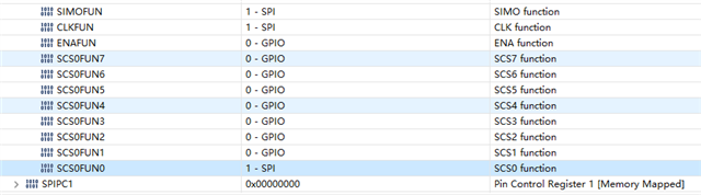
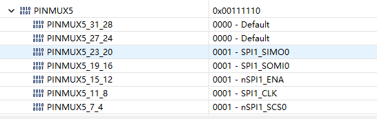
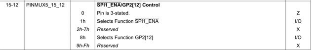
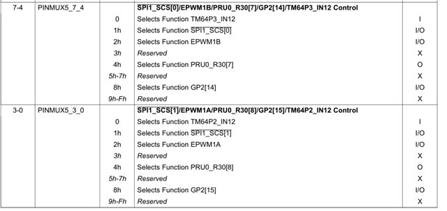
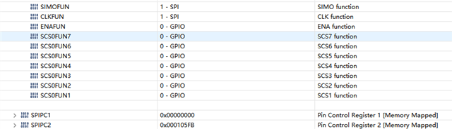
I have just been exposed to TMS320C6748 recently.I now want to write an SPI SLAVE program to receive FPGA data.I found these few sentences in section 28.2.7 of the data manual:

“ In SPI slave mode, the SPIx_SIMO and SPIx_CLK pin output buffer is in a high-impedance state and the SPIx_SOMI pin output buffer is enabled.”

How should I set it to look like a description?

and:"In slave mode with 3-pin option, CPU writes to SPIDAT0[15:0] or SPIDAT1[15:0] makes the slave ready to transmit. CPU writes to the configuration bits in SPIDAT1 (not writing to SPIDAT1[15:0]) do not make the
slave ready to transmit."

I would like to know the difference and connection between SPIDAT1 [15:0] and SPIDAT1.

I really need your help. Thank you.

  • Hello,

    For the first part of your question, the description you provided from the manual indicates that in SPI slave mode, the output buffer for the MOSI (Master Out Slave In) and clock pins is in a high-impedance state, while the MISO (Master In Slave Out) pin output buffer is enabled. To set up your SPI slave program to reflect this description, you would configure the SPI peripheral on the TMS320C6748 to operate in slave mode and ensure that the appropriate pin configurations are set to achieve the desired behavior.

    As for the second part of your question, it mentions the SPIDAT0, SPIDAT1, and their configuration bits. SPIDAT0 and SPIDAT1 are likely the data registers for the SPI peripheral. Writing to SPIDAT0[15:0] or SPIDAT1[15:0] in slave mode with the 3-pin option makes the slave ready to transmit data. However, writing to the configuration bits in SPIDAT1 (without writing to SPIDAT1[15:0]) does not make the slave ready to transmit. This suggests that the configuration bits in SPIDAT1 are separate from the data bits and have a different purpose in the operation of the SPI slave.

    The difference and connection between SPIDAT1[15:0] and SPIDAT1 likely lie in the fact that SPIDAT1 is a wider register that includes both data bits and configuration bits. Writing to the lower 16 bits (SPIDAT1[15:0]) sets the data to be transmitted, while writing to the configuration bits in the upper bits of SPIDAT1 may control aspects of the SPI operation, but do not directly trigger the slave to transmit data.

    To implement this in your program, you would need to understand the specific bit layout of the SPIDAT1 register and ensure that you are writing data and configuration bits to the correct locations within this register.

    Regards,

    Gary

  • I want to know if my understanding is correct:Once I set SPI to SLAVE mode, the sentence "the SPIx_SIMO and SPIx_CLK pin output buffer is in a high-impedance state and the SPIx_SOMI pin output buffer is enabled." has been done?

    I hope you can keep this post open for now, as I have just started learning TMS320C6748 and I cannot find any case programs to learn about SPI_SLAVE, so I can only learn through the user manual. I think I may have some questions about SPI_SLAVE recently and would like to seek your help here. Thank you very much and I need your help. Thank you.

  • Hello,

    I want to know if my understanding is correct:Once I set SPI to SLAVE mode, the sentence "the SPIx_SIMO and SPIx_CLK pin output buffer is in a high-impedance state and the SPIx_SOMI pin output buffer is enabled." has been done?

    Yes, your understanding is correct. When the SPI is set to SLAVE mode, the SPIx_SIMO and SPIx_CLK pin output buffer is in a high-impedance state, and the SPIx_SOMI pin output buffer is enabled. This means that the slave device is ready to receive data on the SPIx_SOMI pin while the SPIx_SIMO and SPIx_CLK pins are in a high-impedance state, allowing the master device to control the communication.

    I hope you can keep this post open for now, as I have just started learning TMS320C6748 and I cannot find any case programs to learn about SPI_SLAVE, so I can only learn through the user manual. I think I may have some questions about SPI_SLAVE recently and would like to seek your help here. Thank you very much and I need your help. Thank you.

    Of course, I'll be happy to answer your questions, as I should, and you're welcome to ask any questions

  • Hello, Gray. As mentioned earlier, I am currently learning SPI and I would like to modify the SPI program in start ware to Slave 3-pin mode to receive data. In Table 28 of the data manual, I found that SCS0FUN needs to be set to 0. After searching for the statement to set it in the program, I was a bit confused. The statement is:
    SPIPinControl (SOC_SPI_1_REGS, 0, 0,&val);
    The specific function is

    void SPIPinControl(unsigned int baseAdd, unsigned int idx,
    unsigned int flag, unsigned int *val)
    {
    if (0 == flag)
    {
    HWREG(baseAdd + SPI_SPIPC(idx)) = *val;
    }
    else
    {
    *val = HWREG(baseAdd + SPI_SPIPC(idx));
    }
    }

    Among them, baseadd(SOC_SPI_1_REGS) is 0X01F0E000, and val's address is 0X00000E01.

    The above figure shows the result of this function on SPIPCP, but according to the table, SCS0FUN should be set to 0. I want to know how I should understand this function and how I should set SCS0FUN to 0.

    I really need your help, thank you.

  • I cannot find the specific function of HWREG and I do not understand how this statement was used to complete the register setting.

  • Based on the function definition, when the `flag` parameter is 0, the function sets the value pointed to by `val` to the specified pin control register. When the `flag` parameter is not 0, the function reads the value from the pin control register and stores it at the address pointed to by `val`.

    To set SCS0FUN to 0 using this function, you would need to do the following:

    unsigned int val = 0; // Set the value to 0 to configure SCS0FUN to 0
    SPIPinControl(SOC_SPI_1_REGS, SCS0FUN_INDEX, 0, &val);

    In this example, `SCS0FUN_INDEX` would be the index corresponding to the SCS0FUN pin control register.

    By calling `SPIPinControl` with the appropriate parameters, you should be able to set SCS0FUN to 0 as required to configure the SPI to operate in Slave 3-pin mode.

  • I understand your confusion. The `HWREG` function is not a standard C function, but rather a macro or inline function typically defined in the header files provided by the manufacturer of the microcontroller or development board. It is often used to access hardware registers directly.

    These registers are memory-mapped, meaning that they can be accessed through specific memory addresses to configure the hardware.

    The `HWREG` function is typically defined to directly access these memory-mapped hardware registers. It is often used in embedded programming to read from or write to hardware registers.

  • Here's an example of how `HWREG` might be defined:

    #define HWREG(x) (*((volatile unsigned int *)(x)))

    This definition creates a macro that can be used to access the hardware registers. When you use `HWREG(baseAdd + SPI_SPIPC(idx))`, it actually translates to accessing the memory location `baseAdd + SPI_SPIPC(idx)` and reading or writing the value at that location.

    In your specific case, when `flag` is 0, the `SPIPinControl` function uses `HWREG(baseAdd + SPI_SPIPC(idx)) = *val;` to write the value pointed to by `val` to the hardware register specified by `idx`. When `flag` is not 0, the function uses `*val = HWREG(baseAdd + SPI_SPIPC(idx));` to read the value from the hardware register and store it at the address pointed to by `val`.

    I hope this helps clarify the usage of `HWREG` and how it is used to complete the register setting in the `SPIPinControl` function. If you have further questions, feel free to ask!

  • Hello Gary,

    I think I understand what you mean: through the HWREG function, we can locate a specific register, and the * val after=in the statement is used to set each corresponding bit of the register.

    void SPIPinControl(unsigned int baseAdd, unsigned int idx,
    unsigned int flag, unsigned int *val)
    {
    if (0 == flag)
    {
    HWREG(baseAdd + SPI_SPIPC(idx)) = *val;
    }
    else
    {
    *val = HWREG(baseAdd + SPI_SPIPC(idx));
    }
    }

    Among them, baseadd(SOC_SPI_1_REGS) is 0X01F0E000, and val's address is 0X00000E00.

    The difference from the original program is that the last bit of the val address changes from 1 to 0, because I found in the data manual that SOS0FUN is the 0th bit, and I successfully set it to 0.

    Thank you very much for your help. I still hope you keep this post open because I really need your help. I think your answers have taught me a lot. You are a great teacher, thank you very much.

  • Hi,

    It doesn't matter, this is what I should do, I will keep this post open, you are welcome to communicate at any time, thank you

    Regards,

    Gary

  • Hello Gary,

    I found this sentence in user manual 28.2.7:

    To select the 3-pin SPI option, the SPIx_CLK, SPIx_SOMI, and SPIx_SIMO pins should be configured as
    functional pins by configuring the SPI pin control register 0 (SPIPC0). The SPIx_SCS[n] and SPIx_ENA
    pins can be used as general-purpose I/O pins by configuring the SPIPC1 through SPIPC5 registers.

    In my current program, they are all set as SPI function pins, and I have found the corresponding program to set them:
    Void GPIOBankPinMuxSet (void)
    {
    SPIPinMuxSetup (1);
    SPI1CSPinMuxSetup (0);
    }
    among
    SPIPinMuxSetup (1)
    Is SPI1 selected;
    SPI1CSPinMuxSetup (0)
    Each bit of SPI1 has been set.
    Specifically:

    void SPI1CSPinMuxSetup(unsigned int csPinNum)
    {
    unsigned int spi1CSPinMux = 0;
    unsigned int savePinMux = 0;

    switch(csPinNum)
    {
    case 0:
    spi1CSPinMux = (SYSCFG_PINMUX5_PINMUX5_7_4_NSPI1_SCS0 << \
    SYSCFG_PINMUX5_PINMUX5_7_4_SHIFT);

    savePinMux = HWREG(SOC_SYSCFG_0_REGS + SYSCFG0_PINMUX(5)) & \
    ~(SYSCFG_PINMUX5_PINMUX5_7_4);
    HWREG(SOC_SYSCFG_0_REGS + SYSCFG0_PINMUX(5)) = \
    (spi1CSPinMux | savePinMux);

    break;

    case 1:
    spi1CSPinMux = (SYSCFG_PINMUX5_PINMUX5_3_0_NSPI1_SCS1 << \
    SYSCFG_PINMUX5_PINMUX5_3_0_SHIFT);

    savePinMux = HWREG(SOC_SYSCFG_0_REGS + SYSCFG0_PINMUX(5)) & \
    ~(SYSCFG_PINMUX5_PINMUX5_3_0);

    HWREG(SOC_SYSCFG_0_REGS + SYSCFG0_PINMUX(5)) = \
    (spi1CSPinMux | savePinMux);

    break;

    case 2:
    spi1CSPinMux = (SYSCFG_PINMUX4_PINMUX4_31_28_NSPI1_SCS2 << \
    SYSCFG_PINMUX4_PINMUX4_31_28_SHIFT);

    savePinMux = HWREG(SOC_SYSCFG_0_REGS + SYSCFG0_PINMUX(4)) &
    ~(SYSCFG_PINMUX4_PINMUX4_31_28);

    HWREG(SOC_SYSCFG_0_REGS + SYSCFG0_PINMUX(4)) = \
    (spi1CSPinMux | savePinMux);

    break;

    case 3:
    spi1CSPinMux = (SYSCFG_PINMUX4_PINMUX4_27_24_NSPI1_SCS3 << \
    SYSCFG_PINMUX4_PINMUX4_27_24_SHIFT);

    savePinMux = HWREG(SOC_SYSCFG_0_REGS + SYSCFG0_PINMUX(4)) & \
    ~(SYSCFG_PINMUX4_PINMUX4_27_24);

    HWREG(SOC_SYSCFG_0_REGS + SYSCFG0_PINMUX(4)) = \
    (spi1CSPinMux | savePinMux);

    break;

    case 4:
    spi1CSPinMux = (SYSCFG_PINMUX4_PINMUX4_23_20_NSPI1_SCS4 << \
    SYSCFG_PINMUX4_PINMUX4_23_20_SHIFT);

    savePinMux = HWREG(SOC_SYSCFG_0_REGS + SYSCFG0_PINMUX(4)) & \
    ~(SYSCFG_PINMUX4_PINMUX4_23_20);

    HWREG(SOC_SYSCFG_0_REGS + SYSCFG0_PINMUX(4)) = \
    (spi1CSPinMux | savePinMux);

    break;

    case 5:
    spi1CSPinMux = (SYSCFG_PINMUX4_PINMUX4_19_16_NSPI1_SCS5 << \
    SYSCFG_PINMUX4_PINMUX4_19_16_SHIFT);

    savePinMux = HWREG(SOC_SYSCFG_0_REGS + SYSCFG0_PINMUX(4)) & \
    ~(SYSCFG_PINMUX4_PINMUX4_19_16);

    HWREG(SOC_SYSCFG_0_REGS + SYSCFG0_PINMUX(4)) = \
    (spi1CSPinMux | savePinMux);

    break;

    case 6:
    spi1CSPinMux = (SYSCFG_PINMUX4_PINMUX4_15_12_NSPI1_SCS6 << \
    SYSCFG_PINMUX4_PINMUX4_15_12_SHIFT);

    savePinMux = HWREG(SOC_SYSCFG_0_REGS + SYSCFG0_PINMUX(4)) & \
    ~(SYSCFG_PINMUX4_PINMUX4_15_12);

    HWREG(SOC_SYSCFG_0_REGS + SYSCFG0_PINMUX(4)) = \
    (spi1CSPinMux | savePinMux);

    break;

    case 7:
    spi1CSPinMux = (SYSCFG_PINMUX4_PINMUX4_11_8_NSPI1_SCS7 << \
    SYSCFG_PINMUX4_PINMUX4_11_8_SHIFT);

    savePinMux = HWREG(SOC_SYSCFG_0_REGS + SYSCFG0_PINMUX(4)) & \
    ~(SYSCFG_PINMUX4_PINMUX4_11_8);

    HWREG(SOC_SYSCFG_0_REGS + SYSCFG0_PINMUX(4)) = \
    (spi1CSPinMux | savePinMux);

    break;

    default:
    break;

    }

    }

    I want to directly set PINMUX5 to the given address earlier, but I don't know how to set other pins except for these SPI pins, which makes it necessary for me to know how the above function works, and then I can modify it to the one mentioned in 28.2.7. It is too difficult for me to ask for your help again. Thank you very much for your help.

  • The function `SPI1CSPinMuxSetup` is used to configure the pin multiplexing for the chip select (CS) pins of SPI1. The specific details of the pin multiplexing setup depend on the hardware and the specific microcontroller or processor you are working with. The code you've shared is manipulating the pin multiplexing registers to configure the SPI pins.

    If you want to directly set the PINMUX5 register to a specific address, it's important to understand the structure and layout of the pin multiplexing registers for your specific hardware. Without that information, it's difficult to provide specific guidance on how to modify the function.

    Could you tell me more about your problem?

  • Sorry gary,I made a mistake. The last function was indeed only about setting SPI1_SCS, and according to the requirements, I should set it to 8. After learning, I have not solved it yet. The function for setting SPI1_ENA is as follows:

    void SPIPinMuxSetup(unsigned int instanceNum)
    {
    unsigned int savePinMux = 0;

    if(0 == instanceNum)
    {
    savePinMux = HWREG(SOC_SYSCFG_0_REGS + SYSCFG0_PINMUX(3)) & \
    ~(SYSCFG_PINMUX3_PINMUX3_3_0 | \
    SYSCFG_PINMUX3_PINMUX3_15_12 | \
    SYSCFG_PINMUX3_PINMUX3_11_8 | \
    SYSCFG_PINMUX3_PINMUX3_7_4);

    HWREG(SOC_SYSCFG_0_REGS + SYSCFG0_PINMUX(3)) = \
    (PINMUX3_SPI0_CLK_ENABLE | PINMUX3_SPI0_SIMO_ENABLE | \
    PINMUX3_SPI0_SOMI_ENABLE | PINMUX3_SPI0_ENA_ENABLE | \
    savePinMux);

    }
    else if(1 == instanceNum)
    {
    savePinMux = HWREG(SOC_SYSCFG_0_REGS + SYSCFG0_PINMUX(5)) & \
    ~(SYSCFG_PINMUX5_PINMUX5_11_8 | \
    SYSCFG_PINMUX5_PINMUX5_23_20 | \
    SYSCFG_PINMUX5_PINMUX5_19_16 | \
    SYSCFG_PINMUX5_PINMUX5_15_12);

    HWREG(SOC_SYSCFG_0_REGS + SYSCFG0_PINMUX(5)) = \
    (PINMUX5_SPI1_CLK_ENABLE | PINMUX5_SPI1_SIMO_ENABLE | \
    PINMUX5_SPI1_SOMI_ENABLE | PINMUX5_SPI1_ENA_ENABLE | \
    savePinMux);
    }
    else
    {

    }

    }

    Where instanceNum=0. But this function is for SPI1_ CLK, SPI1_ SIMO, SPI1_ SOMI, SPI1_ ENA was set together and set them all to 1. According to the requirements of the  3-Pin mode, SPI1_ ENA should be set to 8.

    And I want to know if I need to set both SPI1SCS0 and SPI1SCS1 to 8?

  • Hello Gary, I have discovered a new issue. In our previous discussion, we made the following settings for SPIPC0:

    In these settings, SIMO, SOMI, and CLK are all set to SPI mode, while ENA and SCS are all set to GPIO mode. And now we still need to set the same SPI or GPIO settings for SIMO, SOMI, CLK, ENA, and SCS in PINMUX5. I'm a bit confused about the difference between these two settings? Are there any differences or connections between them?

  • In addition, I have found the exact function to set SPI1_CLK、SPI1_SIMO、SPI1_SOMI、SPI1_ENA:

    // SPI1 pins
    #define PINMUX5_SPI1_CLK_ENABLE (SYSCFG_PINMUX5_PINMUX5_11_8_SPI1_CLK << \
    SYSCFG_PINMUX5_PINMUX5_11_8_SHIFT)

    #define PINMUX5_SPI1_SIMO_ENABLE (SYSCFG_PINMUX5_PINMUX5_23_20_SPI1_SIMO0 << \
    SYSCFG_PINMUX5_PINMUX5_23_20_SHIFT)

    #define PINMUX5_SPI1_SOMI_ENABLE (SYSCFG_PINMUX5_PINMUX5_19_16_SPI1_SOMI0 << \
    SYSCFG_PINMUX5_PINMUX5_19_16_SHIFT)

    #define PINMUX5_SPI1_ENA_ENABLE (SYSCFG_PINMUX5_PINMUX5_15_12_NSPI1_ENA << \
    SYSCFG_PINMUX5_PINMUX5_15_12_SHIFT)

    void SPIPinMuxSetup(unsigned int instanceNum)
    {
    unsigned int savePinMux = 0;

    if(0 == instanceNum)
    {
    savePinMux = HWREG(SOC_SYSCFG_0_REGS + SYSCFG0_PINMUX(3)) & \
    ~(SYSCFG_PINMUX3_PINMUX3_3_0 | \
    SYSCFG_PINMUX3_PINMUX3_15_12 | \
    SYSCFG_PINMUX3_PINMUX3_11_8 | \
    SYSCFG_PINMUX3_PINMUX3_7_4);

    HWREG(SOC_SYSCFG_0_REGS + SYSCFG0_PINMUX(3)) = \
    (PINMUX3_SPI0_CLK_ENABLE | PINMUX3_SPI0_SIMO_ENABLE | \
    PINMUX3_SPI0_SOMI_ENABLE | PINMUX3_SPI0_ENA_ENABLE | \
    savePinMux);

    }
    else if(1 == instanceNum)
    {
    savePinMux = HWREG(SOC_SYSCFG_0_REGS + SYSCFG0_PINMUX(5)) & \
    ~(SYSCFG_PINMUX5_PINMUX5_11_8 | \
    SYSCFG_PINMUX5_PINMUX5_23_20 | \
    SYSCFG_PINMUX5_PINMUX5_19_16 | \
    SYSCFG_PINMUX5_PINMUX5_15_12);

    HWREG(SOC_SYSCFG_0_REGS + SYSCFG0_PINMUX(5)) = \
    (PINMUX5_SPI1_CLK_ENABLE | PINMUX5_SPI1_SIMO_ENABLE | \
    PINMUX5_SPI1_SOMI_ENABLE | PINMUX5_SPI1_ENA_ENABLE | \
    savePinMux);
    }
    else
    {


    }

    }

    It looks like this is an encapsulated function, I want to know
    1.Can I directly modify it?
    2.Can I directly write a new function in the. c and. h files where this function is located to apply the function I wrote in my programming?
    3.How can I set SCS and ENA to GPIO mode?

  • If you need to set SPI1_ENA to 8, it typically means that you want to configure the SPI module in 3-pin mode. In 3-pin mode, you usually have only three pins: SPI_CLK, SPI_SIMO (Slave In Master Out), and SPI_SOMI (Slave Out Master In). In this mode, the SPIENx value of 8 might indicate a specific configuration for 3-pin operation.


    Regarding SPI1SCS0 and SPI1SCS1, these seem to be related to chip selects for the SPI1 module. The requirement to set SPI1_ENA to 8 may be specific to the SPI control register (SPx) and not necessarily related to the chip select values. Chip select values are often determined by the specific device you are communicating with and are not directly related to the SPIENx value.

    To set SPI1_ENA to 8 for 3-pin mode, you should focus on the SPI control register (SPx) associated with SPI1 and not necessarily on the chip select values.

  • 1. SPIPC0 Settings:
    SIMO, SOMI, CLK: These are set to SPI mode, indicating that these pins are configured for SPI communication.
    ENA, SCS: Set to GPIO mode, indicating that these pins are configured as General Purpose I/O (GPIO) pins instead of SPI pins.

    2. PINMUX5 Settings:
    SPI1_CLK, SPI1_SIMO, SPI1_SOMI: Set to SPI mode, indicating that these pins are configured for SPI communication.
    SPI1_ENA (Enable), SPI1_SCS (Chip Select): Set to SPI mode, indicating that these pins are also configured for SPI communication.


    SPI mode and GPIO mode:
    In SPI mode, pins are configured to serve specific functions of the SPI communication protocol, such as serial input/output and clock.
    In GPIO mode, the pins are configured as universal I/O pins, allowing you to use them for any digital input or output.


    Differences between SPI1 and SPI:
    The prefix "SPI1_" in PINMUX5 indicates that these Settings are specific to SPI1.

  • 1. Yes, you can modify the function if you understand the purpose of each line and the intended configuration.

    2. Yes, you can write a new function in the same .c file or include a declaration in the corresponding .h file. Ensure that your new function does not conflict with existing functions or variables in the codebase.

    3. GPIO configuration involves setting the pins to general-purpose digital I/O mode.

  • Hi Gary,

    Based on your guidance, I have made modifications to the program that includes SPIPinMuxSetup. The modified program is as follows:

    void SPIPinMuxSetup(unsigned int instanceNum)
    {
    unsigned int savePinMux = 0;

    if(0 == instanceNum)
    {
    savePinMux = HWREG(SOC_SYSCFG_0_REGS + SYSCFG0_PINMUX(3)) & \
    ~(SYSCFG_PINMUX3_PINMUX3_3_0 | \
    SYSCFG_PINMUX3_PINMUX3_15_12 | \
    SYSCFG_PINMUX3_PINMUX3_11_8 | \
    SYSCFG_PINMUX3_PINMUX3_7_4);

    HWREG(SOC_SYSCFG_0_REGS + SYSCFG0_PINMUX(3)) = \
    (PINMUX3_SPI0_CLK_ENABLE | PINMUX3_SPI0_SIMO_ENABLE | \
    PINMUX3_SPI0_SOMI_ENABLE | PINMUX3_SPI0_ENA_ENABLE | \
    savePinMux);

    }
    else if(1 == instanceNum)
    {
    savePinMux = HWREG(SOC_SYSCFG_0_REGS + SYSCFG0_PINMUX(5)) & \
    ~(SYSCFG_PINMUX5_PINMUX5_11_8 | \
    SYSCFG_PINMUX5_PINMUX5_23_20 | \
    SYSCFG_PINMUX5_PINMUX5_19_16 | \
    SYSCFG_PINMUX5_PINMUX5_15_12);

    HWREG(SOC_SYSCFG_0_REGS + SYSCFG0_PINMUX(5)) = \
    (PINMUX5_SPI1_CLK_ENABLE | PINMUX5_SPI1_SIMO_ENABLE | \
    PINMUX5_SPI1_SOMI_ENABLE | PINMUX5_SPI1_ENA_ENABLE | \
    savePinMux);
    }

    else if(2 == instanceNum)
    {
    savePinMux = HWREG(SOC_SYSCFG_0_REGS + SYSCFG0_PINMUX(5)) & \
    ~(SYSCFG_PINMUX5_PINMUX5_11_8 | \
    SYSCFG_PINMUX5_PINMUX5_23_20 | \
    SYSCFG_PINMUX5_PINMUX5_19_16 | \
    SYSCFG_PINMUX5_PINMUX5_15_12);

    HWREG(SOC_SYSCFG_0_REGS + SYSCFG0_PINMUX(5)) = \
    (PINMUX5_SPI1_CLK_ENABLE | PINMUX5_SPI1_SIMO_ENABLE | \
    PINMUX5_SPI1_SOMI_ENABLE | PINMUX5_SPI1_GPIO_ENABLE | \
    savePinMux);
    }


    else
    {


    }

    }

    #define PINMUX5_SPI1_CLK_ENABLE (SYSCFG_PINMUX5_PINMUX5_11_8_SPI1_CLK << \
    SYSCFG_PINMUX5_PINMUX5_11_8_SHIFT)

    #define PINMUX5_SPI1_SIMO_ENABLE (SYSCFG_PINMUX5_PINMUX5_23_20_SPI1_SIMO0 << \
    SYSCFG_PINMUX5_PINMUX5_23_20_SHIFT)

    #define PINMUX5_SPI1_SOMI_ENABLE (SYSCFG_PINMUX5_PINMUX5_19_16_SPI1_SOMI0 << \
    SYSCFG_PINMUX5_PINMUX5_19_16_SHIFT)

    #define PINMUX5_SPI1_ENA_ENABLE (SYSCFG_PINMUX5_PINMUX5_15_12_NSPI1_ENA << \
    SYSCFG_PINMUX5_PINMUX5_15_12_SHIFT)

    #define PINMUX5_SPI1_GPIO_ENABLE (SYSCFG_PINMUX5_PINMUX5_15_12_GPIO2_12 << \
    SYSCFG_PINMUX5_PINMUX5_15_12_SHIFT)

    #define SYSCFG_PINMUX5_PINMUX5_11_8_SHIFT (0x00000008u)
    #define SYSCFG_PINMUX5_PINMUX5_11_8_SPI1_CLK (0x00000001u)

    #define SYSCFG_PINMUX5_PINMUX5_23_20_SHIFT (0x00000014u)
    #define SYSCFG_PINMUX5_PINMUX5_23_20_SPI1_SIMO0 (0x00000001u)

    #define SYSCFG_PINMUX5_PINMUX5_19_16_SHIFT (0x00000010u)
    #define SYSCFG_PINMUX5_PINMUX5_19_16_SPI1_SOMI0 (0x00000001u)

    #define SYSCFG_PINMUX5_PINMUX5_15_12_SHIFT (0x0000000Cu)
    #define SYSCFG_PINMUX5_PINMUX5_15_12_NSPI1_ENA (0x00000001u)
    #define SYSCFG_PINMUX5_PINMUX5_15_12_GPIO2_12 (0x00000008u)

    Logically speaking, the program I modified should be able to change the ENA bit to GPIO, but the actual result of the program running is exactly the same as before. I think this may be a problem with library calls? Perhaps the function library I modified is not the one called by the main function? But currently it seems that I cannot find any other function libraries that include SPIPinMuxSetup. For the modification of SPIPinMuxSetup, I made it directly in the Notepad program. I want to know where I can view the function library called by the main function? Or could you provide me with some ideas?

  • Sorry Gary,

    The last time it was possible that there was a problem with the software, and I tried to restart the software to run the program. I found that the running result turned into the following image:

    What is the reason for this? This result is incorrect for instanceNum equal to 0 or 1 or 2.

  • I can give you some suggestions to help you debug and find the source of the problem:

    1. View the main features:
    First look at the main function in your program. Verify that the correct instance number is passed to the 'SPIPinMuxSetup' function. Make sure the instance number is 0, 1, or 2, as expected in the code.

    2. Check function calls:
    Look for the point in your code where 'SPIPinMuxSetup' is called. Verify that the correct instance number is passed as a parameter. Make sure that the changes you make to 'SPIPinMuxSetup' are reflected in all instances that call it.

    3. Search for other instances of the function:
    If you suspect that another version of this function may exist in the codebase, perform a global search for 'SPIPinMuxSetup' in all project files. This will help you determine if the function has multiple definitions.

    4. Check the function declaration:
    Make sure that the declaration of 'SPIPinMuxSetup' matches the modified definition. The declaration usually appears in the header file (.h). Verify that the function prototype matches the definition and includes the correct header files where needed.


    5. Print debugging statement:
    Insert a print or debug statement in 'SPIPinMuxSetup' to log a message indicating when it is called and the value of the associated variable. This helps you track the execution process and identify any unexpected behavior.

    6. Verify memory write:
    Make sure that the memory location written in 'SPIPinMuxSetup' is correct. Verify that the values to be written to these locations are as expected.

  • 1. Memory Corruption:
    Ensure that you are not inadvertently overwriting memory outside the bounds of your variables or arrays. Check for buffer overflows or uninitialized memory usage.

    2. Pointer Issues:
    Verify that your pointer usage is correct. Incorrect dereferencing of pointers or accessing invalid memory locations can lead to unpredictable behavior.

  • In addition, if you have other new questions, please post again and exchange, I will continue to answer for you, I will close this post, thank you for understanding, thank you