Other Parts Discussed in Thread: TDA4VM
HI expert:
There has some questions about TDA4VL OSPI read and write:
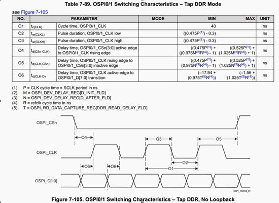
The OSPI of TDA4VL was configured as Tap DDR mode. During the signal test, it was found that the Timing Requirements could be met, but the Switching Characteristics timing could not be met.
The software configuration is as follows:
P = CLK cycle time = SCLK period in ns = 20.75MHz ——ns:1/20.75*1000=48.19ns
M = OSPI_DEV_DELAY_REG[D_INIT_FLD] = 10
N = OSPI_DEV_DELAY_REG[D_AFTER_FLD]=10
R = refclk cycle time in ns = 166MHz——ns:1/166*1000=6ns
T =OSPI_RD_DATA_CAPTURE_REG[DDR_READ_DELAY_FLD] = 0
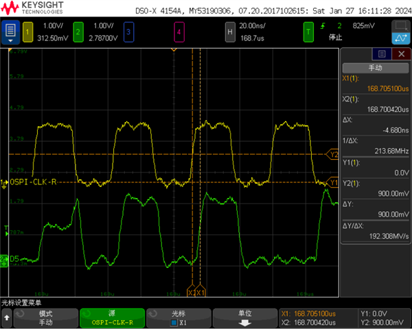
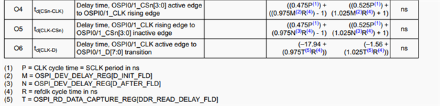
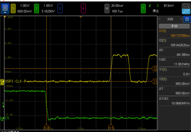
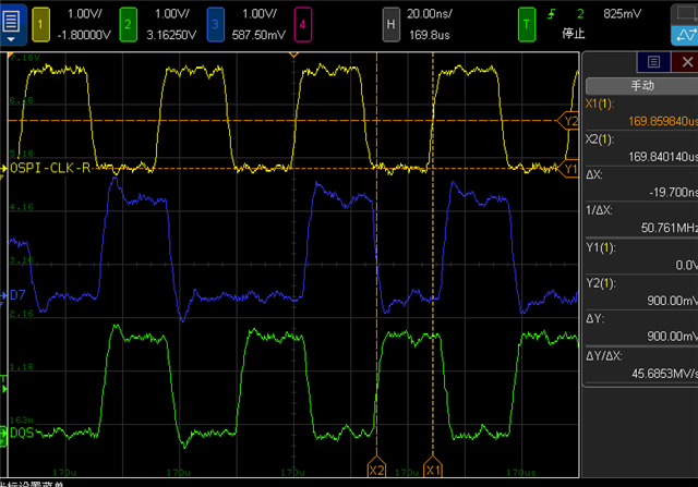
Using the above data and TDA4VL-Q1 to calculate O4 O5 O6, the results are as follows. The measurement timing cannot meet the requirements, but the communication is OK.See those test pictures:
|
O4 |
td(CLK-CSn) |
Delay time, CSn active edge to CLK rising edge |
1.8V |
0.475 * P +0.975 * M * R- 1 (2) (3) (5) |
80.3915665 |
0.525 * P +1.025 * M * R+ 1(2) (3) (5) |
82.80120505 |
ns |
|
O5 |
td(CLK-CSn) |
Delay time, CLK rising edge to CSn inactive edge |
1.8V |
0.475 * P +0.975 * N * R- 1(2) (4) (5) |
80.3915665 |
0.525 * P +1.025 * N * R+ 1 (2) (4) (5) |
82.80120505 |
ns |
|
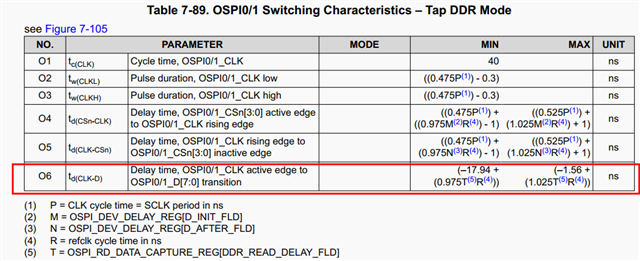
O6 |
td(CLK-D) |
Delay time, CLK active edge to D[i:0] transition(1) |
1.8V, OSPI0 DDR TX; 1.8V, OSPI1 DDR TX |
-17.94 + 0.975*T*R |
-17.94 |
-1.56 + 1.025*T*R |
-1.56 |
ns |
Two questions need to be answered:
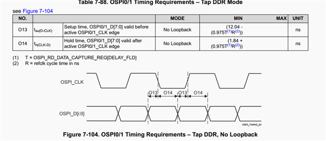
① Does OSPI read refer to the Switching Characteristics sequence?
② The result calculated by the formula is too large, is it the problem of the formula?(I compared the TDA4VM specification, there is no such formula, and the parameters are not calculated to be so large)
Timing:
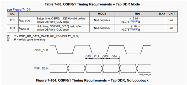
Switching Characteristics: