This thread has been locked.
If you have a related question, please click the "Ask a related question" button in the top right corner. The newly created question will be automatically linked to this question.
DRV401和DRV421芯片框架图太过简化,无法理解磁通门信号如何转为补偿线圈电流信号,请问有相关资料项目描述内部电路或功能模块,以便于设计人员能够设计外围电路,完成产品设计?激励线圈产生的正负PWM信号如何转为补偿线圈的电流信号?
您好,
对于 DRV401-EP,很抱歉我们仅有的资料是其 datasheet:https://www.ti.com.cn/cn/lit/ds/symlink/drv401-ep.pdf
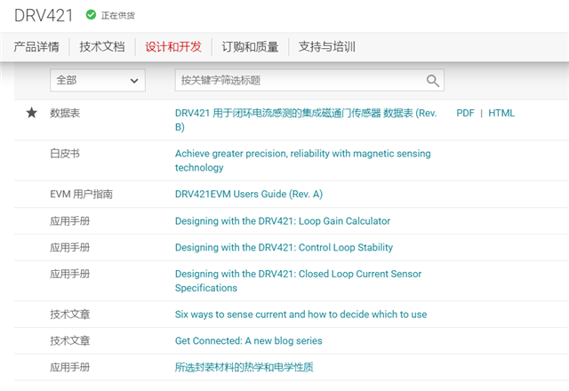
对于DRV421,在其产品主页(https://www.ti.com.cn/product/cn/DRV421 )还提供了以下文档:
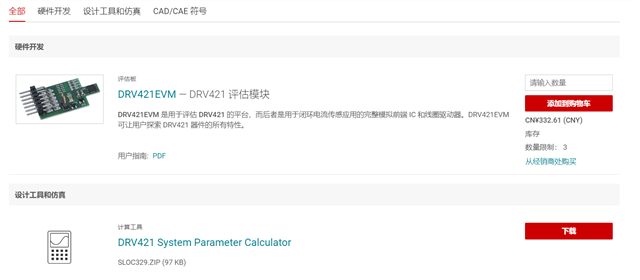
以及 DRV421EVM和计算工具:
另外,也建议您在E2E英文支持论坛,检索已得到解答的相关问题,或发帖咨询资深的英文论坛工程师:
https://e2e.ti.com/search?q=DRV421&category=forum