If you have a related question, please click the "Ask a related question" button in the top right corner. The newly created question will be automatically linked to this question.
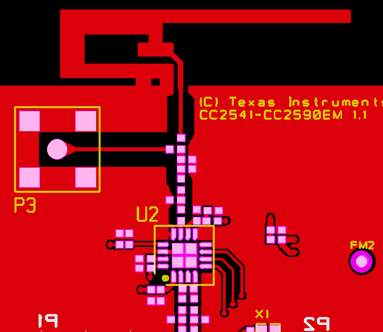
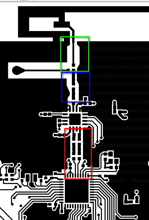
PCB DESCRIPTION:4 LAYER PCB 1.6 MM Copper 1 35 um Dielectric 1-2 0.175 mm (e.g. 1x Prepreg 7628 AT05 47% Resin) Copper 2 18 um Dielectric 2-3 1.14 mm (6x 7628M 43% Resin) Copper 3 18 um Dielectric 3-4 0.175 mm (e.g. 1x Prepreg 7628 AT05 47% Resin) Copper 4 35 um DE104iML or equivalent substrate (Resin contents around 45%, which gives Er=4.42@2.4GHz, TanD=0.016) Dimensions in mil (0.001 inch) DOUBLE SIDE SOLDER MASK, DOUBLE SIDE SILKSCREEN, 8 MIL MIN TRACE WIDTH AND 5 MIL MIN ISOLATION.