

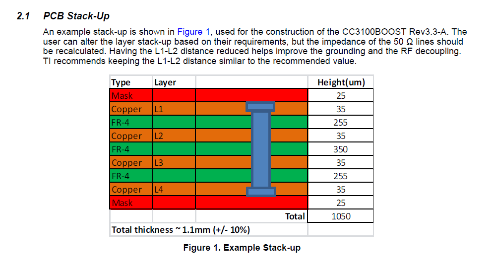
An example stack-up is shown in Figure 1, used for the construction of the CC3100BOOST Rev3.3-A. The
user can alter the layer stack-up based on their requirements, but the impedance of the 50 Ω lines should
be recalculated. Having the L1-L2 distance reduced helps improve the grounding and the RF decoupling.
TI recommends keeping the L1-L2 distance similar to the recommended value.