

Other Parts Discussed in Thread: CC2592
1、如下这两个芯片间信号线为差分线吗,具体特性阻抗应该控制多少;
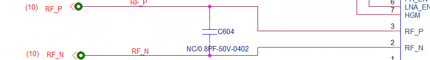
2、CC2592规格书中对GND要求“Only terminals 9, 11, and 12 should be shorted to the die attach pad on the top PCB layer“
,但是其他GND脚没有说明,参考设计里是全部与低部PAD相连了,我们按照参考设计即可吗
Other Parts Discussed in Thread: CC2592
1、如下这两个芯片间信号线为差分线吗,具体特性阻抗应该控制多少;
2、CC2592规格书中对GND要求“Only terminals 9, 11, and 12 should be shorted to the die attach pad on the top PCB layer“
,但是其他GND脚没有说明,参考设计里是全部与低部PAD相连了,我们按照参考设计即可吗


