Part Number: UC2845
Dear TI Support Team,
I am currently designing a Flyback converter using the UC2845 PWM controller. I am encountering some abnormal behaviors during the startup phase and would appreciate your professional insights.
System Specifications:
-
Controller: UC2845
-
Switch: MOSFET (1500V, 2.5A)
-
Target Output: 24V Adaptor
-
Vcc Source: External 15V DC Supply (for testing purposes)
-
Gate Resistor (Rg): 260 ohms
Issues Observed:
-
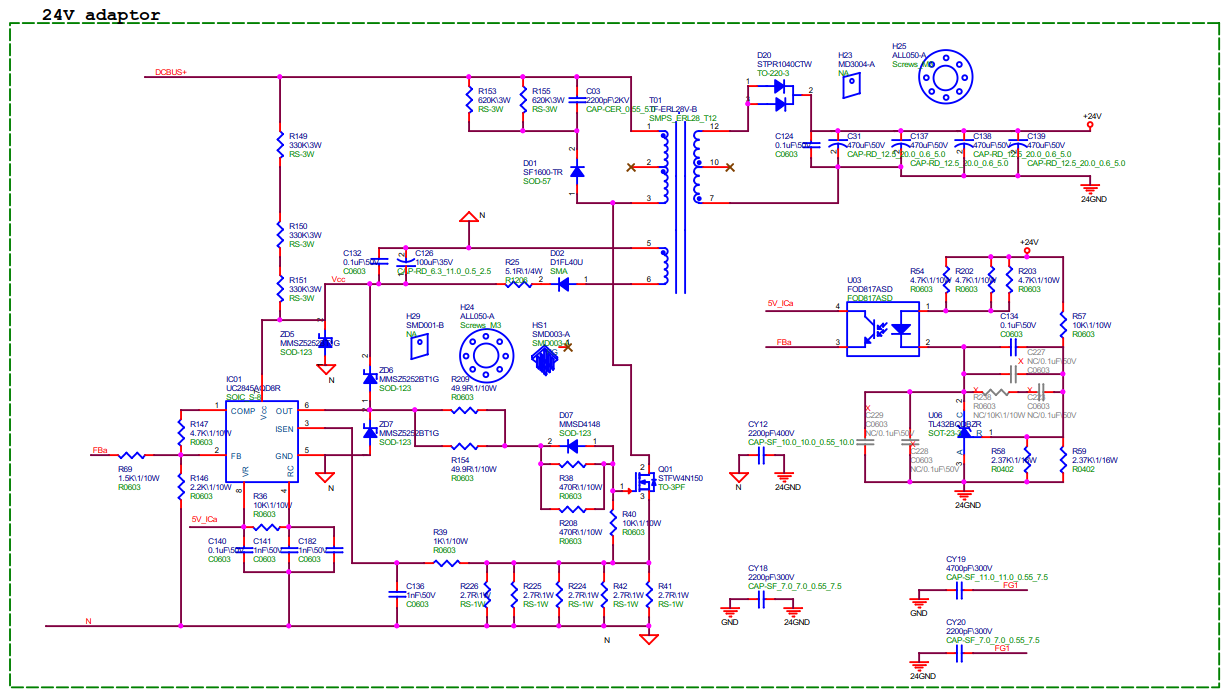
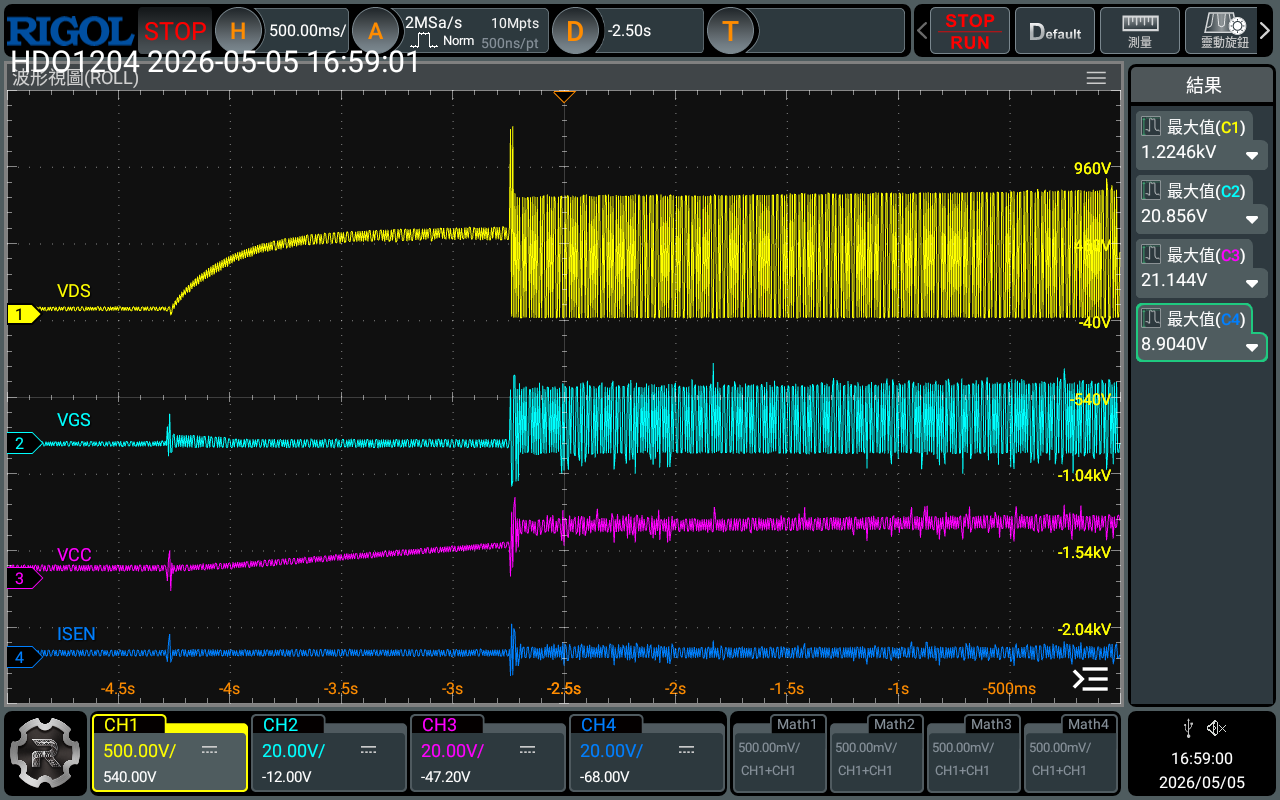
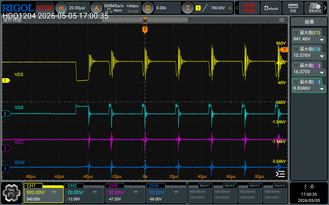
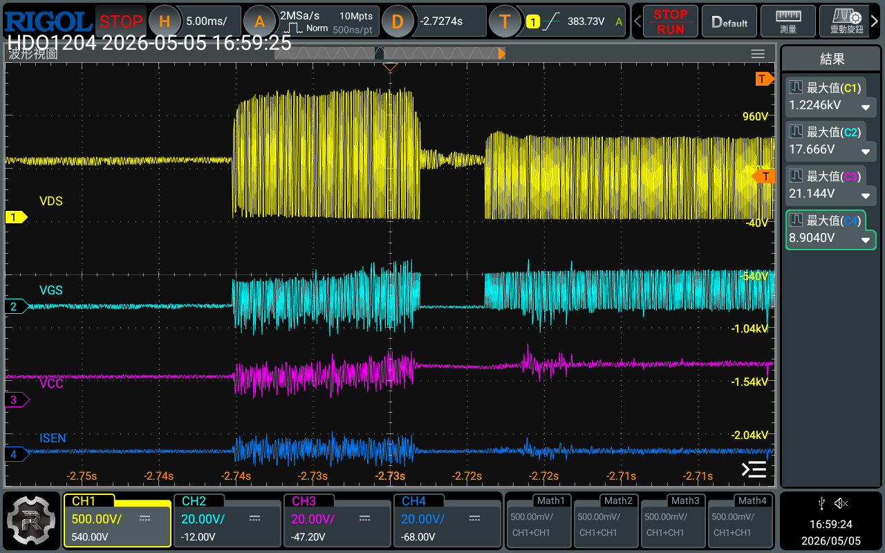
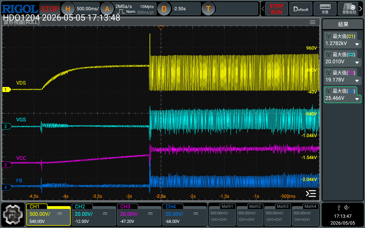
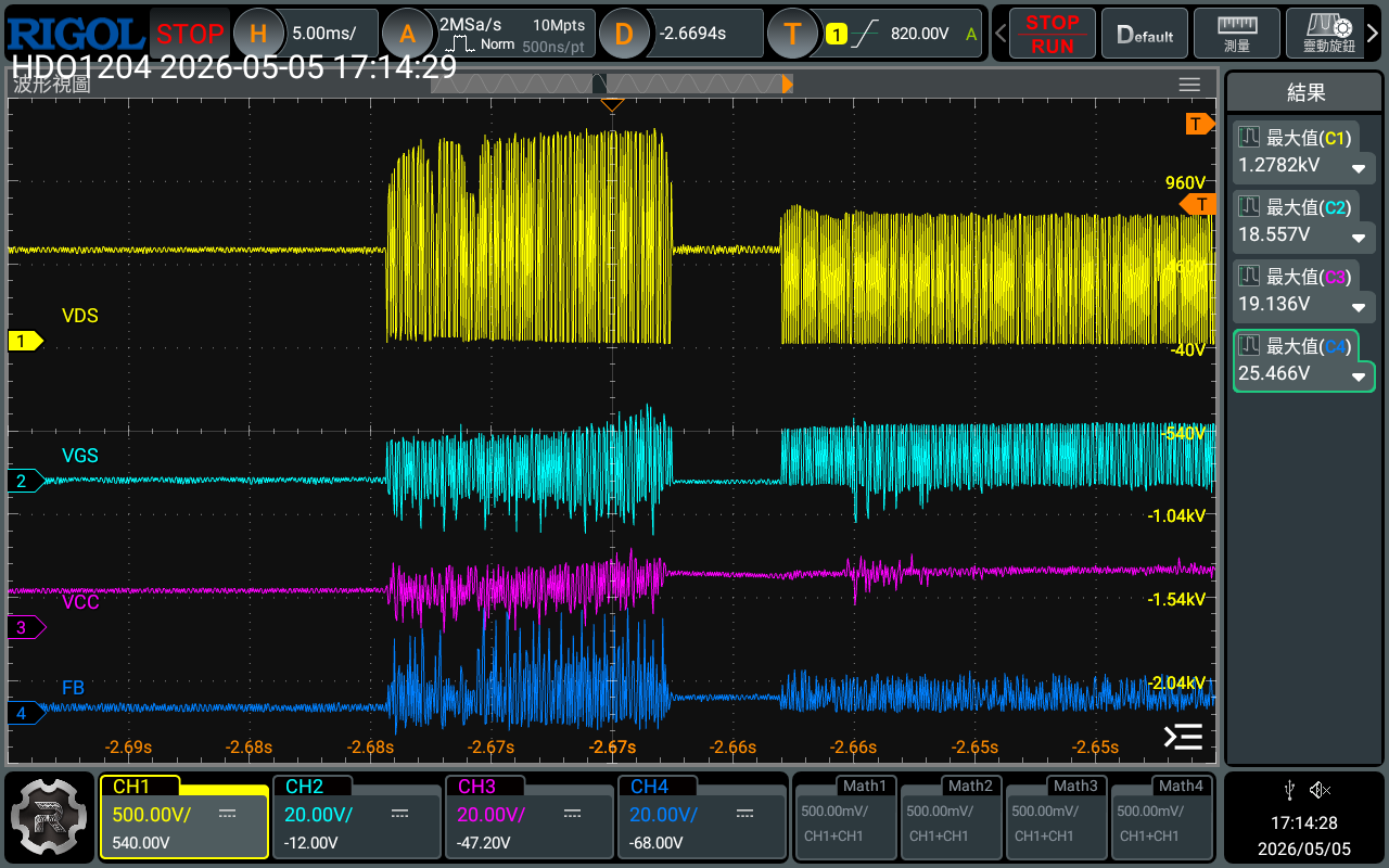
Startup Hiccup (Blanking Period): Even with a stable external 15V Vcc, there is a significant "blanking period" (approx. 50-100ms) where the PWM output stops before restarting. I suspect it might be related to the ISEN (Pin 3) protection being triggered by inrush current or noise.
-
Gate Drive Distortion: As shown in the attached waveforms (CH2: VGS), the gate drive signal is severely distorted with heavy ringing. The peak VGS is lower than expected, and the MOSFET seems to struggle to fully enter the linear (ohmic) region, staying too long in the saturation region.
-
High Voltage Spike: The VDS spike reaches 1.4kV, which is very close to the MOSFET's 1.5kV rating.
Experimental Setup & Attachments:
-
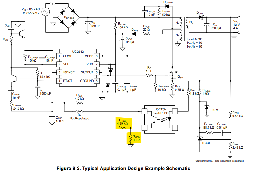
Schematic: Full circuit diagram of the Flyback converter.
-
Test Condition: Please note that for the attached waveforms, I have connected two additional resistors (same ohmic value as the original) in parallel within the RCD Snubber network to evaluate the impact on the VDS spike.
-
Waveforms: Oscilloscope captures showing VDS, VGS, VCC, FB and ISEN signals during startup.
-
CH1 (Yellow): VDS (showing the 1.25kV spike)
-
CH2 (Cyan): VGS (showing drive distortion)
-
CH3 (Purple): VCC
-
CH4 (Blue): FB or ISEN
-
Questions:
-
What could be the primary cause of the long blanking period despite a stable Vcc?
-
Based on the schematic, are there any recommendations for the ISEN filter (RC) or Gate Drive circuit to improve signal integrity and reduce ringing?
-
Do you recommend any specific adjustments to the RCD Snubber or Soft-start to mitigate the 1.4kV startup spike?
Thank you for your time and assistance. I look forward to your reply.
Best regards,
JIANWEI WU
新代科技/台灣新代 SYNTEC