Other Parts Discussed in Thread: TPS63710
TPS63710(WSON封装) 在AD中布线时显示中间的地上的四个焊盘,clearence constraint<0mil between pad on mulitylayer and pad on top layer。那么该如何布地线呢?还有在datesheet中四个是VIA不是PAD啊,官网上下载的模型怎么会是pad呢?
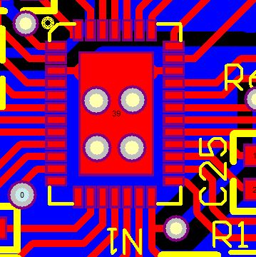
Other Parts Discussed in Thread: TPS63710
TPS63710(WSON封装) 在AD中布线时显示中间的地上的四个焊盘,clearence constraint<0mil between pad on mulitylayer and pad on top layer。那么该如何布地线呢?还有在datesheet中四个是VIA不是PAD啊,官网上下载的模型怎么会是pad呢?