

Part Number: OPA858DSGEVM
Other Parts Discussed in Thread: OPA858
 Dear Engineer, I wo
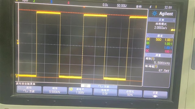
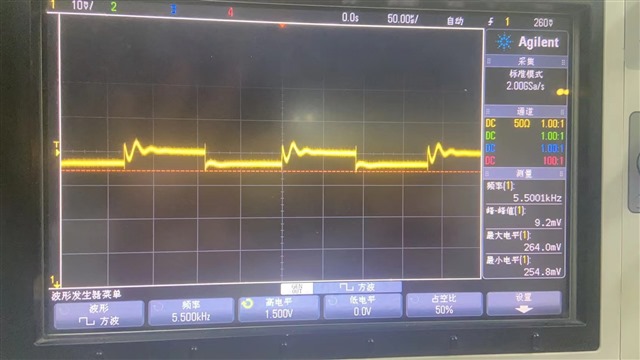
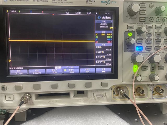
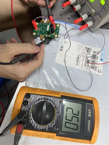
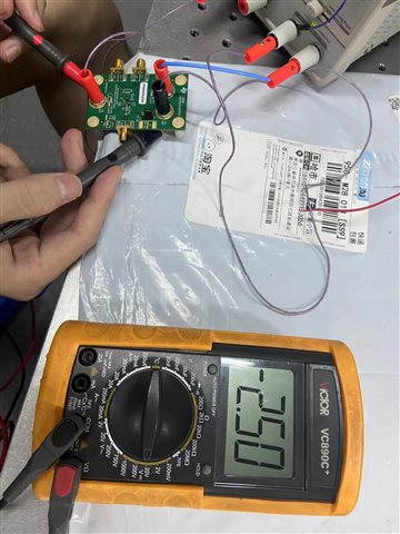
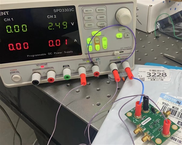 uld like to consult you regarding an issue. I previously purchased an OPA858DSGEVM evaluation module. At first, when I applied a signal to the inverting input, the circuit did not work. After checking the schematic, I suspected that the 0-ohm resistor R3 connected to ground might have been the reason, because it directly routed the input signal to ground, preventing it from entering the amplifier. Later, I removed R3. Then, without connecting VCC or VEE, I applied a square wave signal generated by an oscilloscope to the inverting input. The signal had a minimum value of 0V and a maximum of 0.5V, and the output voltage showed a Vpp of 34mV. When I increased the square wave amplitude to 0V–1V, the output Vpp became 67.5mV. When the square wave amplitude was 1.5V, the output maximum value was 87.7mV and the minimum was 8.8mV. This made me feel that the amplifier might have started working, because before removing R3, applying a square wave would not produce any square-like signal at the output. Next, I tried dual power supply, e.g., VCC=2.5V and VEE=-2.5V, but the output instead showed only 10mV or 20mV of voltage swing. Later, I switched to a single supply configuration with VCC=5V and VEE=0V, but the output was still the same. After reading the OPA858 Op Amp EVM User’s Guide, I noticed there are restrictions on dual-supply operation, such as maximum and minimum VCC-VEE values and allowable input voltage ranges. Therefore, I set VEE=0.4V and VCC=3V, and configured the square wave signal with a low level of 1V and a high level of 1.01V, but the output still only showed Vpp of 10mV or 20mV, which is far from the expected gain of 7. I wonder if my device might be damaged. The first attached waveform shows the output when there was no VCC or VEE supply and the input signal had a high level of 1V and a low level of 0.5V. The second waveform shows the output with VEE=1V, VCC=3V, and input signal levels of 0V (low) and 1.5V (high). The third waveform shows the output with input high at 1.01V and low at 1V. Afterwards, I powered the board with ±2.5V without applying any input or connecting the output, and the power supply showed a current of 0.01A, as seen in images 4, 5, and 6. I hope to get your advice on this. Thank you!

