

我从TINA里导入了2N6755模型,有三个问题:1.模型沟道宽度1.1m,TINA里默认模型是不是设置错了。 2.这里面有G-S overlap capacitance,是不是代表我导入了模型,这个模型已经默认设置好gate和drain之间有寄生电容。 3.请问有没有射频电磁场对芯片干扰的仿真或者资料可以让我学习下。 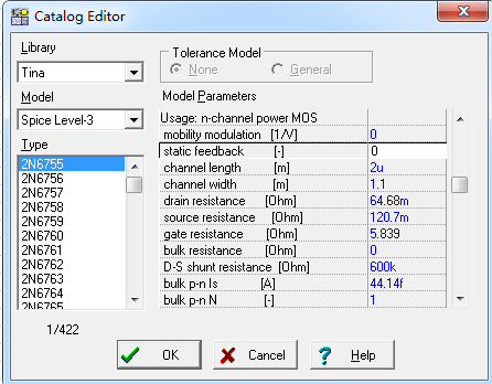
我从TINA里导入了2N6755模型,有三个问题:1.模型沟道宽度1.1m,TINA里默认模型是不是设置错了。 2.这里面有G-S overlap capacitance,是不是代表我导入了模型,这个模型已经默认设置好gate和drain之间有寄生电容。 3.请问有没有射频电磁场对芯片干扰的仿真或者资料可以让我学习下。
