While this design may still yield acceptable results in the application, it is a simple matter to adjust these
resistor values slightly to get perfect gain match from the two output currents to the amplifier output and
also provide exactly the same apparent resistive load to each output. Implementing this adjustment also
moves in the direction of giving better channel linearity and, therefore, lower distortion. Achieving matched
gain magnitudes also moves the mid-scale DC output (when both output currents are equal to IP/ 2)
closer to 0V at the op amp output. The designs here assumed bipolar supplies for the op amp where a 0V
output is desired when each DAC channel is at (I
P
/ 2) (midscale). While there might be other, more
dominant, distortion mechanisms that mask this improvement, it is preferable to remove this unmatched
output voltage swing as a possible source of imbalance.
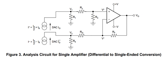
To balance this design, start with the full design circuit of Figure 3, and write the gain and input impedance
equations looking into each port. Define the desired gain as G (which will be an impedance) and input
impedance Ζ
i
(which will also be an impedance).这是opa695datesheet的一段话,对应图,谁能告诉我 输入端的ip.iB分别指什么啊?
