


Part Number: BUF802
设计参数按照BUF802DATASHEET 的11.2章节进行了设计,输入端口为高阻配置
测试输入端口S21参数如下图1所示,测试点为经过C26以后的高频部分:
The design parameters are designed in accordance with section 11.2 of BUF802DATASHEET, and the input port is high resistance configuration
The parameters of the test input port S21 are shown in Figure 1 below, and the test point is the high-frequency part after C26
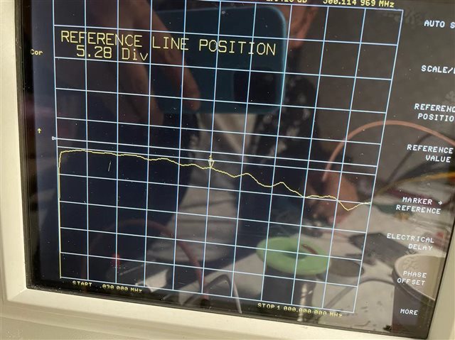
图1信号端口到C26后的S21曲线
Figure 1 Curve of S21 after signal port to C26
测试输出端口经过一个50欧姆的电阻后信号高频部分S21曲线如下图所示:
After the test output port passes a 50 ohm resistance, the S21 curve of the high frequency part of the signal is shown as the figure below:
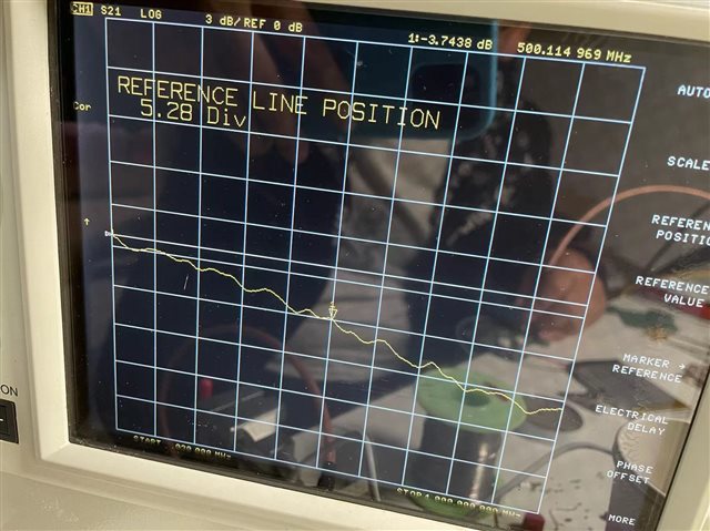
图2 输出端口S21曲线
Figure 2 Curve of output port S21
为什么测试输出端-3dB带宽差距如此大?
Why is the test output -3dB bandwidth gap so big?
目的是想调成-3dB带宽1Ghz的高阻抗输入链,原理图设计如下图3所示
The purpose is to adjust the high-impedance input chain with a bandwidth of -3dB and 1Ghz. The schematic design is shown in Figure 3 below
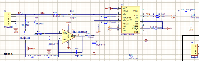
图3 buf802设计的原理图
FIG. 3 Schematic diagram of buf802 design
