
Part Number: THS4561
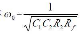
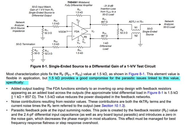
in THS4561 datasheet,the 1th page,the picture below is the demo shematic of butterworth fillter.in this circuit,how to caculate it's cut-off frequency?i found use F=1/(2*PI*sqrt(R1*C1*R2*C2)) can't get correct value.thanks a lot!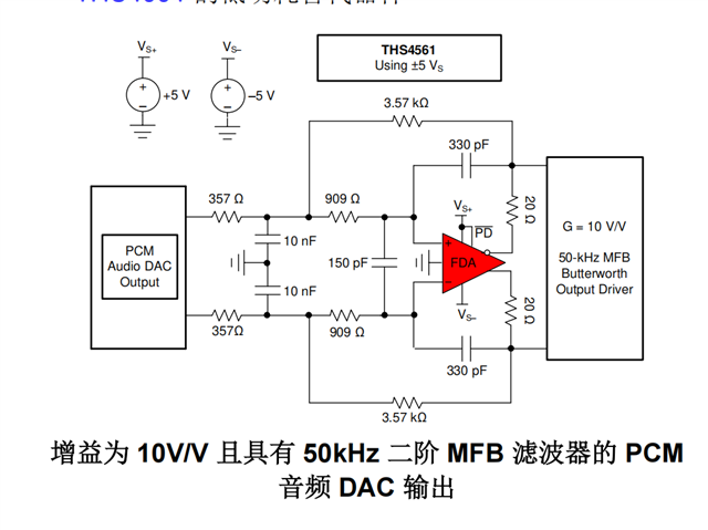

 ,
,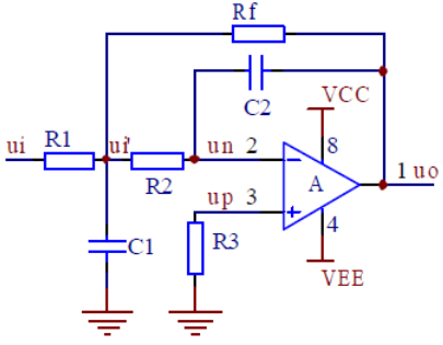
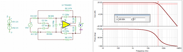
 这个条件,但仿真博德图截止频率大约是20K左右并不是40Khz,是什么问题?图中放大2.5倍,博德图增益7.86db,截止频率4.86db处是20K左右.辛苦解答!
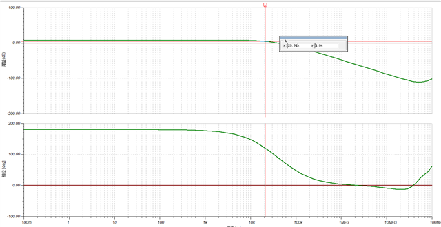