AWR1642 PCB 板载天线设计


TI工程师,你好:

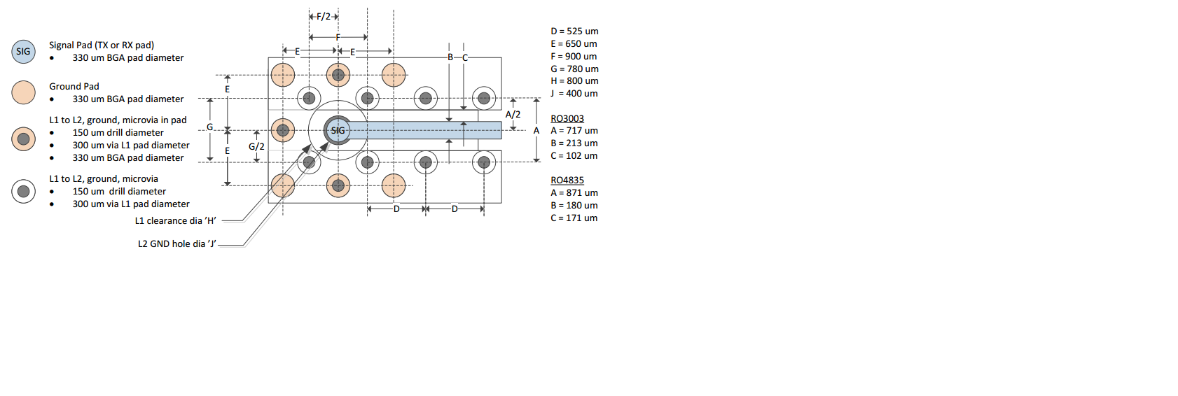
   我最近在看AWR1642的雷達設計,天線部分是把AWR1642BOOST上面的天線給copy過來的。

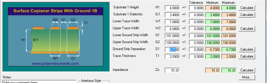
但是最近在算天線50ohm阻抗控制的時候,發現用TI官網上面資料所給出的值計算出來的阻抗并不是

標準的50ohm,而是51ohm,我想請教一下這種設計是否合理?阻抗計算的表如下:

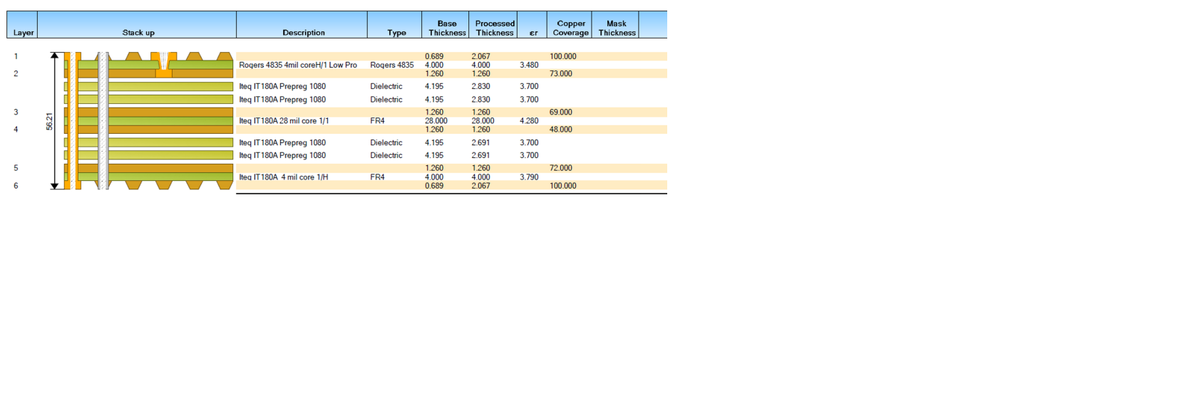
叠构图计阻抗计算如下,望不吝賜教,非常感謝!

  • 你好,

    此处设计要求为50欧。不能完全参考stack-up文件/rogers材料手册中的DK值(非77GHz下测量得到的)。需要借助仿真工具进行仿真,理由如下:

    RF traces are designed to 50 Ohm impedance with the GCPW topology using Rogers Material. 

    Do not refer to the Dk values present in the stack-up as a requirement of controlled impedance for the RF traces.

    These numbers are not accurate and they don't calculate Dk values at mmWave frequencies, also there are many other factors that affects the Dk value such as topology used, surface roughness, type of Cu used, operating frequency etc...   

    Typically these are comprehended in 3D EM simulator (Such as Ansys HFSS, CST or any equivalent 3D EM simulator) tools and from that PCB geometry's are optimized to get 50 Ohm transmission line impedance matching. You could refer to below "TI mmWave Radar sensor RF PCB Design, Manufacturing and Validation Guide" app-note" for more detail, page 3 provides the dimensions for the RF traces. 

    http://www.ti.com/lit/an/spracg5/spracg5.pdf

    It's important to hit the GCPW Dimensions as mentioned in the application note, that ensures required impedance. These values are derived from 3D EM simulator.

    You could mention in the FAB note to adhere to these targeted dimensions for the PCB fabricator.  

    Dk value given in the stack-up is a notional value (Typically it's stated for a lower frequency), Dk value De-rates across frequency. 

    For Antenna simulations, it's best to use the Dk value given by Roggers calculator. 

    For Trace width/Air gap calculations we need to rely upon 3D EM geometry and solver than planar solver present in the Roggers calculator. 
    Geometry dimension shown in the table is arrived after 3D EM simulation. 

    谢谢

  • Hi Wesley

    Thanks for your reply. You mean that the Dk value I used is not correct, can i ask PCB vender to help provide Dk value or calculate it by myself? By the way, can you kindly tell me what are the parameters "Base thickness" and "Processed thickness"show in stackup mean? which one should be used for impedance calculate?
    Best Regards!