This thread has been locked.

If you have a related question, please click the "Ask a related question" button in the top right corner. The newly created question will be automatically linked to this question.

TAS5825M: PVDD供电,DVDD悬空会有电压

Part Number: TAS5825M

Hi ti team,

我们新项目在使用TAS5825M,当PVDD供电时,DVDD悬空,此时DVDD为什么会有电压输出?如果这是正常现象,请问当PVDD供电时,DVDD电压输出能关掉吗?

  • 您好,

    当PVDD供电时,DVDD悬空,此时DVDD为什么会有电压输出?

    芯片正常工作,需要PVDD和DVDD都供电。

    它们是相互独立的路径,无上电时序要求,理论上这种情况不应该出现。

    如果只有PVDD供电,没有DVDD供电,也不会损坏芯片。

    电源路径如图所示,

    TAS5805M: Disable DVDD and keep PVDD 19V in power down application - Audio forum - Audio - TI E2E support forums

  • Hi  Alice,

    我们验证了TAS5825MEVM,发现当只给PVDD=22V供电(DVDD悬空),DVDD会有2.68V电压输出,请帮忙核实下,Thanks!

  • 您好,

         请提供原理图,并说明一下测试过程。

  • Hi Alex,

    客户把TAS5825M的J2和J3跳线帽拿掉(图1),让后给PVDD供电22V,这时DVDD电压显示2.68V(图2)。

    图1

    图2

  • Hi Alice,

    请帮忙确认下这个问题?Thanks!

  • 您好,

         和相关的专家重新确认了一下,他的回复如下,请参考:     

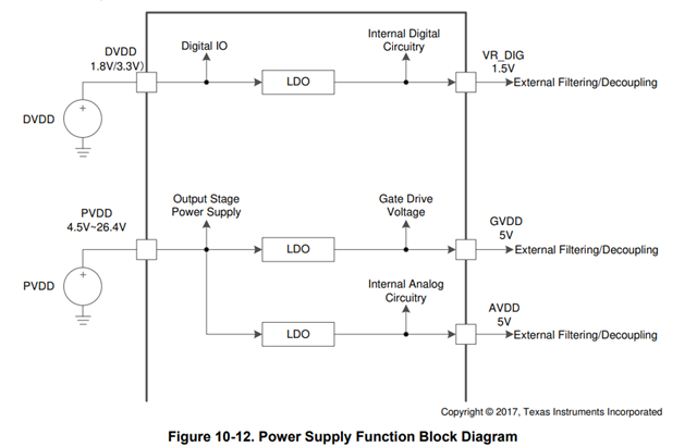
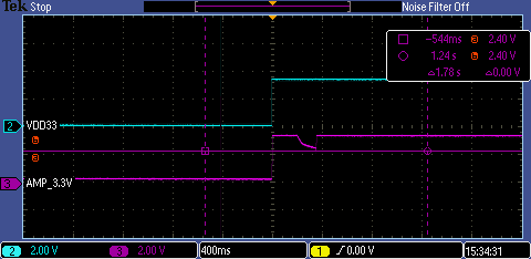
    When DVDD is floating while PVDD is powered, voltage might "couple" or "leak" to the DVDD pin from PVDD via parasitic diodes, leakage currents, or protection circuits (like ESD diodes) inside the chip.
    The measured 2.68V is likely a "clamped voltage" formed through an internal protection diode (e.g., a clamp diode from PVDD to DVDD) or a parasitic path – a parasitic conduction phenomenon when the chip is not fully powered down.

    Never leave DVDD floating! Its level must be actively controlled.

    The phenomenon you observed (2.68V at DVDD when PVDD=22V and DVDD is floating) is due to unintended voltage coupling caused by internal parasitic paths or protection diodes in the chip. Strictly speaking, this is not the chip's 'normal operating state' but rather a 'parasitic conduction' phenomenon occurring under non-standard power sequencing.
    To ensure system stability and chip safety, we strongly recommend avoiding a floating DVDD in the design. We suggest adding a 100kΩ ~ 1MΩ pull-down resistor to the DVDD pin. 

  • Hi Alice,

    我们有按照原厂的建议在DVDD上增加100K和330K的下拉电阻测试,发现DVDD这个凹陷依旧还是存在的,没有变化,如左图。然后我们也翻阅了TAS5825M的规格书PVDD和DVDD对上电时序的要求,规格书中说的是PVDD和DVDD之间无时序要求。我们的本意是想弄清楚即使是DVDD会被PVDD通过内部钳位倒灌回来,但DVDD的这个塌陷是什么造成的?

  • 您好,

         即使增加了100K / 330K下拉电阻,电压“没有变化”。这表明:
    1. 下拉电阻不足以“拉低”由内部二极管钳位建立的电压(当内部二极管导通时,它表现为低阻抗路径)。
    2. 或者,芯片的内部寄生电容/路径在上电过程中会产生瞬态电压下降,而慢速下拉电阻无法及时响应。

    这种“下降”不是稳态电压,而是在上电瞬间的瞬态现象。即使稳态电压为2.68V,由于电容放电或路径切换,瞬时电压仍可能下降。