Part Number: CDCI6214
Other Parts Discussed in Thread: TICSPRO-SW, CDCE6214
Hi everyone,
We are trying to use the CDCI6214 to multiply a 10MHz OCXO output to 100MHz for our FPGA.
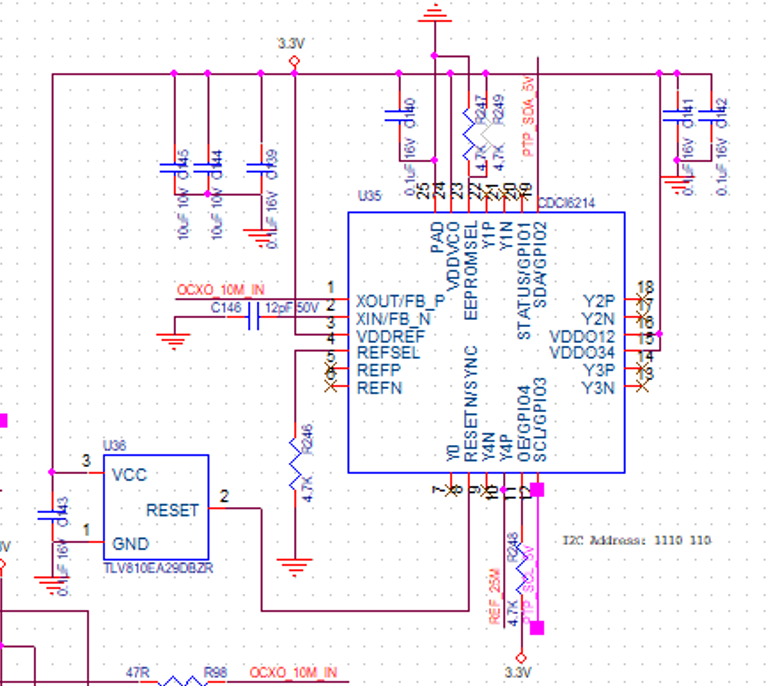
Hardware Setup:
-
Pin 1: 10MHz square wave from the OCXO.
-
Pin 2: 12pF 50V capacitor to GND.
-
Pin 3: 3.3V supply.
-
Pin 4: Pulled to GND via a 4.7k resistor.
-
Pins 5 & 6: Left floating.
-
Pin 8: Connected to a reset IC.
-
Pins 12 & 19: Connected to the host I2C bus.
(I've attached our current schematic for reference.)
Issues Encountered: We found that the reset IC wasn't working properly, and Pin 11 doesn't support single-ended output. To work around the reset issue, we removed the reset IC and manually pulled Pin 8 low during power-up to satisfy the chip's power-up timing requirements.
After doing this, we can successfully read and write configurations via I2C from the host.
Current Goal & Configuration: We want to use the simplest possible configuration just to get the chip working and verify the signal path from input to output before moving on to further debugging. Our current register configuration is:
Addr Op Value
0x01 write 0x6A22
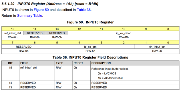
0x1A write 0x0B01
0x1B write 0x0001
0x1D write 0x4032
0x05 write 0x0000
0x00 write 0x0004
wait 1 second
0x07 read -> 0x0C10
We’ve tried several other configuration combinations, but whenever we read Register 0x07, the result is always 0x0C10.
Could anyone provide some advice or suggestions on how to troubleshoot and resolve this issue?
Thanks in advance!