This thread has been locked.
If you have a related question, please click the "Ask a related question" button in the top right corner. The newly created question will be automatically linked to this question.
(2) LMX2594: LMX2594:手动ramp模式出现许多杂波 - 时钟和计时论坛 - 时钟和时序 - E2E 设计支持 (ti.com)
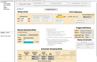
For waveforms that are NOT calibration free, the slew rate of the ramp must be kept less than 250 kHz/µs. Also,
for all automatic ramping waveforms, be aware that there is a very small phase disturbance as the VCO crosses
over the integer boundary, so one might consider using the input multiplier to avoid these or timing the VCO
calibrations at integer boundaries.
对于不是免校准的波形,斜坡的压摆率必须保持小于 250 kHz/µs。 此外,对于所有自动斜坡波形,请注意当 VCO 越过整数边界时会出现非常小的相位干扰,因此可以考虑使用输入乘法器来避免这些或在整数边界处对 VCO 校准进行定时。
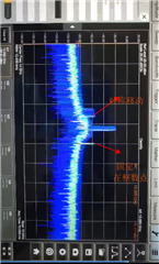
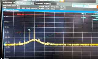
对于手动RAMP出现的在整数倍鉴相FPD频率处出现的杂波是否是相位干扰,(整数边界杂散),这对于连续性的相位是否有影响,而且此处的杂波是一根在整数倍fpd出现,还有一根在主信号另外一侧对称出现。
E2E论坛工程师已给出回复:
Can we get the programming that's being used to generate this screenshot?
I suspect the spurs seen at multiples of FPD are phase detector spurs; there should be some effect on their amplitude when reducing charge pump current or loop bandwidth. But another cause may exist depending on the specific programming.
There should only be an effect on the phase during ramping if the N-divider increments or decrements (in other words, if an integer boundary is crossed in the feedback path). As long as the integer portion of the N-divider remains constant, no phase hit should be observed.
Again, it would help a lot if we can get the programming used to generate this screenshot.
对应的中文是:
是否可以给出用于生成此截图的编程?
我怀疑在 FPD 倍数处看到的杂散是相位检测器杂散;在降低 charge pump current 或 loop bandwidth 时,应对其幅度产生一定影响。 但另一个原因可能存在,具体取决于具体的编程。
只有当 N 分频器增加或减少时(换言之,如果反馈路径中的整数边界被交叉),在ramping 期间相位才会受到影响。 只要 N 分频器的整数部分保持不变,就不应出现相位干扰。
再次,如果能够给出用于生成此截图的编程将非常有帮助
E2E工程师反馈:
Couples of reason:
1. Fractional spurs
Since fpd = 100MHz but the ramp step is 1MHz. At 10000MHz output, there is no spurs. But when you ramp the frequency between 10001MHz and 10099MHz, you will see fractional spurs. These spurs are unavoidable because the PLL is in fractional mode.
2. Ramp clock spurs
if we continue to sweep the frequency, this is equivalent to frequency modulate the PLL, in other words, we are doing FM modulation. As a result, there will spurs (modulation) equal to the modulation frequency (= ramp clock frequency). Higher ramp clock frequency will push the spurs frequency to a higher offset frequency and as a result, lower spurs.
3. VCO calibration
You have the ramp threshold set to 30MHz, since ramp step is 1MHz, so there will be a VCO calibration every 30MHz ramp is elapsed. During VCO calibration, there will be unwanted spurs or glitches. If the ramp range is less than 100MHz, maybe we can sweep the frequency without a VCO calibration, but this calibration-free range is not guarantee.
几个原因:
1.小数杂散
由于 fpd = 100MHz,但 ramp step 为1MHz。 在10000MHz 输出时,不存在任何 spurs。 但是,当您将频率提高到10001MHz 到10099MHz 之间时,您将看到小数杂散。 这些杂散是不可避免的,因为 PLL 处于分数模式。
2.Ramp 时钟杂散
如果我们继续扫频,这相当于频率调制 PLL,换句话说,我们正在进行 FM 调制。 因此,将产生等于调制频率(=ramp 时钟频率)的杂散。较高的ramp 时钟频率会将杂散频率推至较高的偏移频率,从而降低杂散。
3. VCO 校准
您将ramp threshold设置为30MHz,因为ramp step 为1MHz,因此每经过30MHz ,都会进行 VCO 校准。 在 VCO 校准过程中,将出现意外的杂散或杂波。 如果ramp 范围小于100MHz,我们可以在没有 VCO 校准的情况下扫频,但这一免校准范围不能保证。