Part Number: CDCE62005
你好,我想用我自己的电路初始化和编程CDCE62005。但是现在我有一些问题。
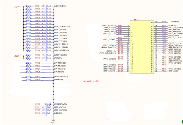
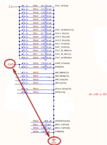
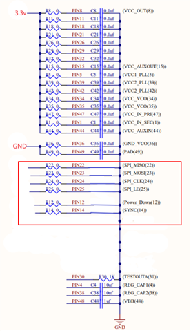
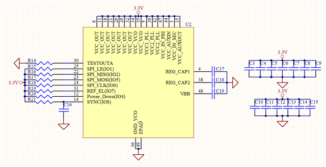
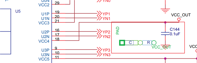
首先,我不确定构建的芯片外围电路是否正确,我无法确认芯片是否工作,也没有办法在芯片手册中验证芯片的正常运行。请帮我检查一下我的电源电路是否正确,引脚配置是否正确。
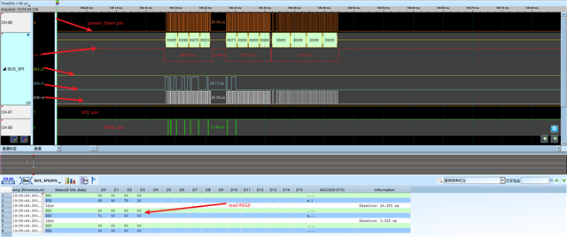
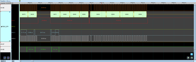
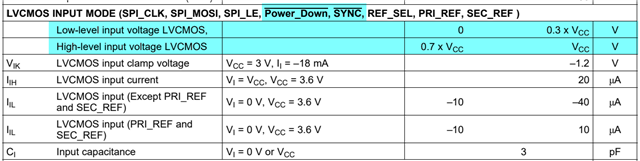
其次,在芯片上电后,我去读寄存器8,返回的数据都是零。我使用模式0的spi时序,/power_down引脚和/sync引脚悬空,但我测量它们的功率电平是逻辑0。
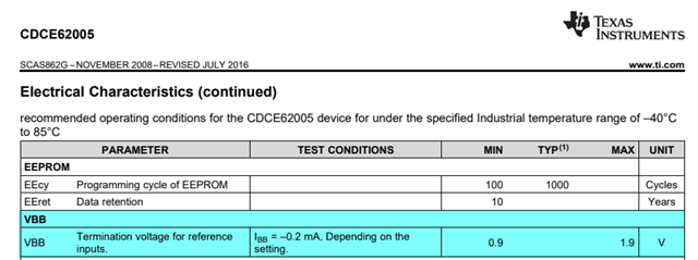
根据数据表,芯片上电(vcc给入后,无需拉高拉低power_down引脚),完成power_on_reset操作后,会自动进入校准保持模式,其中spi->ON,所以我认为/program /sync /rel引脚不需要控制。因为我只需要在芯片的ram和eeprom上操作,这个配置正确吗?