


Part Number: CDCLVC1310
Hi TI
The following picture is the schematic diagram of our project, please help to confirm whether there is any problem,thanks ~
Figure 1 :The single -end signal from TCXO output is fed into CDCLVC1310 PRI_INP as a reference CLK;
Figure 2 : CDCLVC1310 circuit;
and Whether unused signal pins(XIN/XOUT,SEC_INN/INP) can be float ?
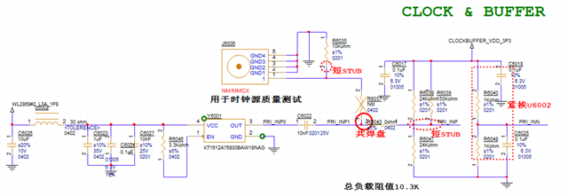
Figure 1
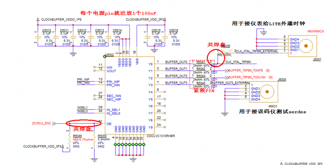
Figure 2