ADS7853:Abnormal issue with SPI reading CFR register of ADS7853

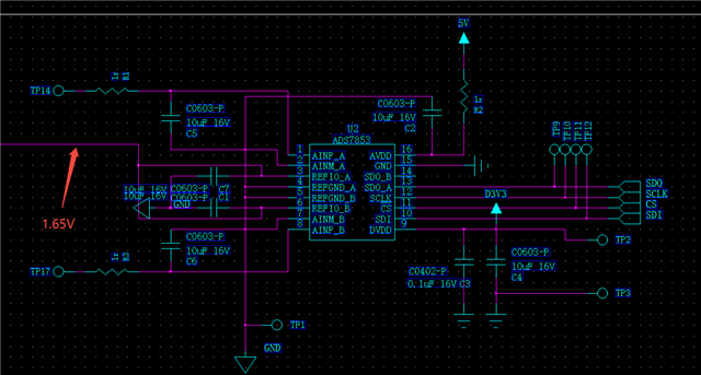
Other Parts Discussed in Thread: ADS7853

Hi, Experts,

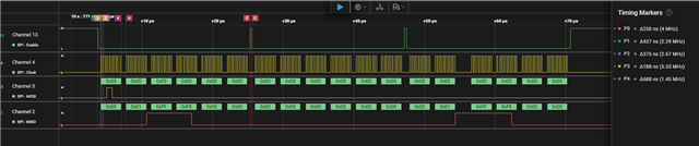
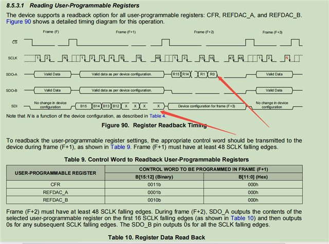
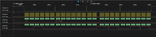
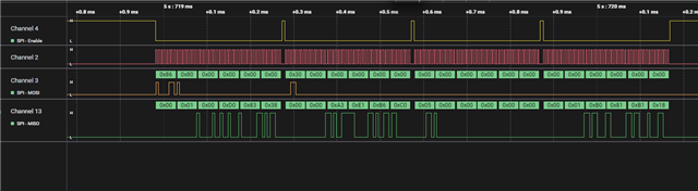
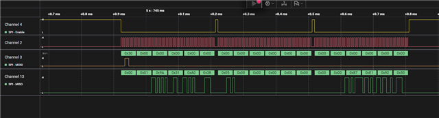
I have a problem with the communication process. When I communicate with ADS7853 using SPI, I am unable to read data correctly form the CFR register, and there are exceptions during setup. The document states that during frame (F+2), SDO-A will return the configuration value of the CFR register. Reality, there is no data return. What is happening? Moreover, after modifying the CFR register again, there was no change in re reading the register. Has anyone experienced the same problem as me.How should we solve it.
............

  • 感谢您对TI产品的关注。
    我们正在核实您的问题,请等待我们的答复。

  • 请问是否能提供你们自己读取时参数时的逻辑分析仪的波形或数据呢?

  • 目前没有找到您想要的波形或者数据,这款芯片还是基于数据手册里面的内容。

    您目前的情况,我们再帮您看一下,有结果会回复到本贴。

  • 你们是否在真实的芯片中进行测试呢,是否是正常的呢?因为,我即使采用模拟的SPI尽可能的按照手册的内容进行读取配置和配置ADS7853芯片,但是,还是无法在读取配置(0X3000)读到返回的前十六位即frame(F+2)中返回的正确数据。

  • 能否请您提供一张类似的截图,展示写入命令以及CFR寄存器的配置方式?
    从这张图像来看,CFR寄存器似乎未配置。由于第1帧(F+1)包含ADC数据,而F+2帧全为00(默认CFR配置),F+3帧又重复了相同数据,这表明系统可能在执行某种寄存器读回指令。
    您能否确认ADCA的输入是什么?接近满量程吗?能否也提供一份原理图?REFIO的电压是多少?


  • 通过设置后还是会无法得到正确的数据的,例如上面这两个,而且每100ms重新访问CFR得到的F+2帧的数据也并不是一个稳定的数据即高16bit数据,但是,大概率都是0X0D00,或0x0500的可能性比较大

  • 是否能帮忙提供你们测试配置ADS7853为32bit单通道的示波器波形图,或csv文件或逻辑分析仪或其他等得到的波形呢,可以让我们进行对比差异在哪,而且我也在你们官网查过ADS7853的原理图似乎没啥大的区别。

  • I noticed some things: 

    1. The command 0x8680 is writing to the CFR register, it is setting bits:
      1. CFR.B10 & CFR.B9 --> RD_DATA_LINES to SDO_A only which is good & INPUT_RANGE = 2xVREF
      2. CFR.B7 --> INM_SEL = 1 --> "1 = INM must be externally connected to the FSR_ADC_x / 2 potential"
        1. in your schematic I noticed you have the INM pins shorted to ground. 
        2. This could cause some issues when reading back data. 
    2. The external REFIO voltage on the schematic says 1.65V, the ADS7853 input vref value should be between 2.4V to AVDD (5V)
      1. This could also be causing issues. 
      2. Could this voltage be set to 2.5V or something within the limits? 
    3. In the data transaction screen shots it appears that the device is recognizing the read register command (0x3000..), in the next frame the logic analyzer appears to incorrectly read what was written before (0x680)
      1. If you look at the actual square wave the 1st pulse looks longer that the 2nd. If the logic analyzer was adjusted that would be the 0x0680 that was written to the device. 
      2. Could the logic analyzer be adjusted to recognize the correct data. the SDI data gets latched on falling edge and the SDO launches data after the falling edge (read data on rising edge)