DAC39RF10: The Issue of Whether the Bias Voltage Will Damage the DAC39RF10 During Power-Up

Part Number: DAC39RF10
Other Parts Discussed in Thread: LMH5401

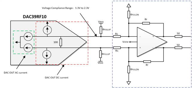
Hello, in my project, the output interface of the DAC39RF10 adopts a design that uses DC coupling and interfaces with a fully differential operational amplifier (FDA).The circuit design refers to the document in the link below.《DAC38RF8x+LMH5401_interface》

DAC38RF82EVM: DAC38RF82EVM questions - Data converters forum - Data converters - TI E2E support forums


According to the datasheet, the compliance voltage range of the DAC is 1.3V~2.3V.
I set the Vbias voltage to 5V so that the DC bias is 1.8V. However, the datasheet states that the voltage range of the DAC's analog output pin is -0.3V~2.3V.
During the power-up phase, when the DAC is in an unconfigured state, the voltage of the DAC's analog pin will exceed 2.3V. Will this cause damage to the DAC?
If this situation needs to be avoided, is it necessary to set Vbias as a segmented voltage? That is, during the power-up phase, when the DAC is unconfigured, set Vbias to 2.3V, and after the DAC is configured, adjust Vbias to 5.0V?