

Part Number: ADS9224R
Other Parts Discussed in Thread: TS5A3159
Hello, I've encountered some issues while designing and using the ADS9224, and I'd like to describe them to you in detail. First, my schematic design is as follows:
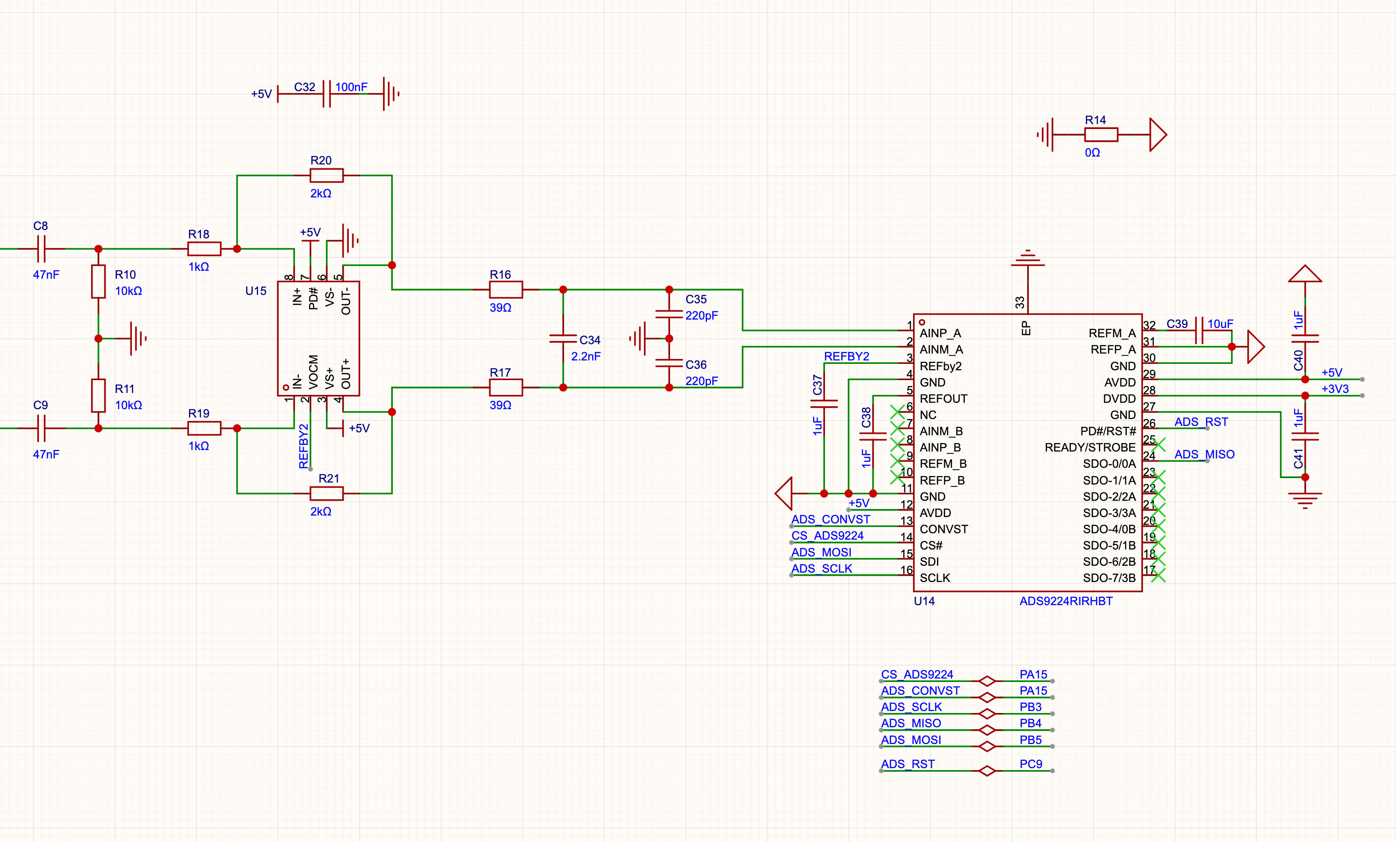
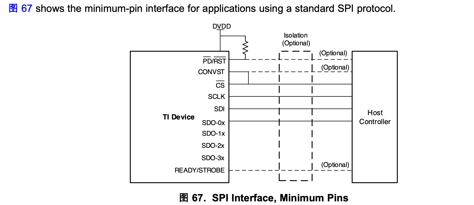
In my design, I referred to the description on page 40 of the datasheet: "Single Device: Minimum Pins for a Standard SPI Interface." I'm using an STM32H5, which can generate the correct read timing in this circuit design. However, I have a concern regarding this reference design: when writing to the ADS9224 registers, I found that CONVST must be pulled high. Yet, in this reference design, CONVST is tied directly to CS. Does this design potentially mislead users, as it seems impossible to configure the registers under such a connection?
Although I am unable to configure the registers, the default initial configuration largely meets my requirements. I then used the STM32 HAL function HAL_SPI_Receive(_cfg.spi, (uint8_t*)pData, Size, Timeout); to receive data and successfully obtained readings. After uploading this data to a host PC for observation, I found that the displayed values do not match my actual measurements.
In my setup, I connected the two leftmost pins in the schematic together and tied them to GND. Theoretically, after passing through the subsequent signal conditioning circuitry, the input to the ADC should be 0 V. However, the data I acquired consistently shows values such as 0x08E3 (≈ −0.927 V), 0x10E3 (≈ −0.926 V), and 0x0CE3 (≈ −0.926 V). This indicates that the ADC is indeed capturing a DC signal, but with a significant offset error.
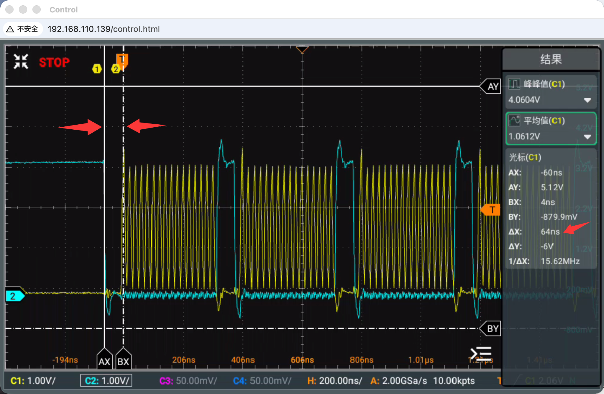
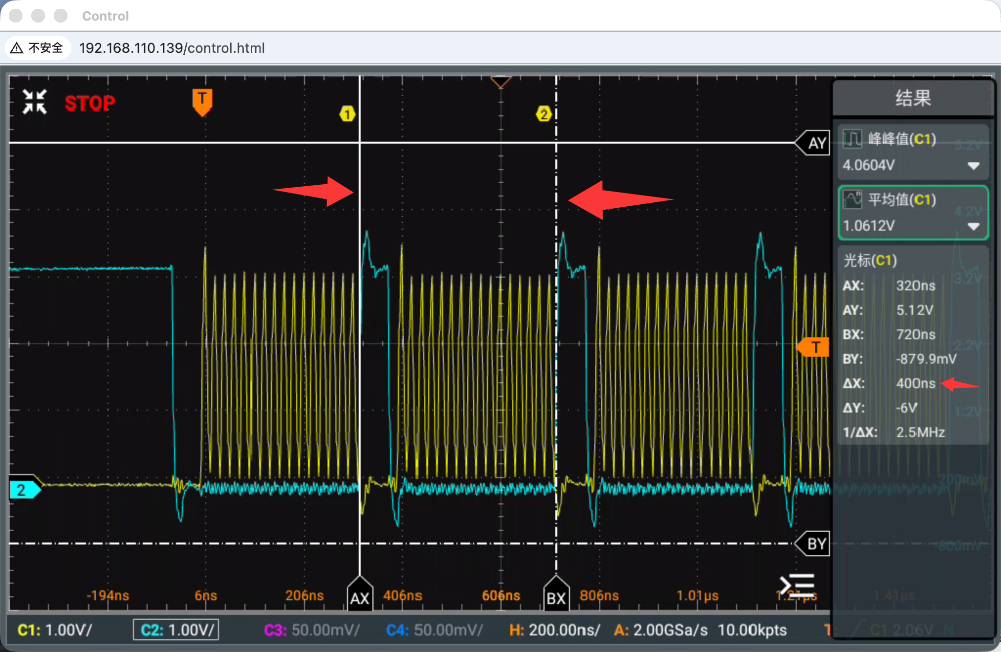
The figure below shows the timing diagram of the acquired data (Zone 2 mode). I think I might have identified the issue—the default register configuration is probably not set to Zone 2—but I’ll continue describing my problem first.
As can be seen, the timing for conversion and data reading is correct. With CONVST tied to CS, pulling CS high triggers the conversion.
I captured 100 data points, as listed below. The data exhibits a continuous and uninterrupted steady-state characteristic, but it is not at 0 V.
Moreover, I also captured the SDO waveform, which matches the data received by the host PC. By the way, I'm using an STM32H5 microcontroller, which operates in little-endian mode.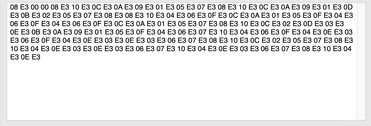
I also measured the input voltage at the ADC front end with a multimeter—black probe connected to GND and red probe to the input—and both channels read approximately 2.38 V, which is close to REF/2. This raises another question for me: why isn’t it around 2.048 V? I also measured the REFOUT voltage, which is about 2.498 V.
I'm confused about the discrepancy between my measurements and the expected values—could you please offer some suggestions? Additionally, I find the minimal pinout design shown on page 40 somewhat misleading, as it appears impossible to configure the device registers with that setup.
I would greatly appreciate an official response from Texas Instruments.
Sincerely,
A student from Xidian University


