Part Number: DAC8551
Other Parts Discussed in Thread: OPA189, OPA828,
Hello everyone,
I am designing a high-precision analog front-end for measuring small voltage variations. The system includes an instrumentation amplifier, a DAC-based dynamic offset cancellation stage, a fixed-gain difference amplifier, a programmable gain stage, and a high-speed SAR ADC.
The issue I am seeing is that once the DAC offset path is connected to the fixed-gain difference amplifier, the input-referred RMS noise increases from a few µV to about 30–40 µV RMS. More interestingly, even when the inputs of the DAC offset amplifier are both tied to AGND, so that its output should ideally be 0 V, the noise is still almost the same as when the full DAC offset circuit is connected.
1. System structure
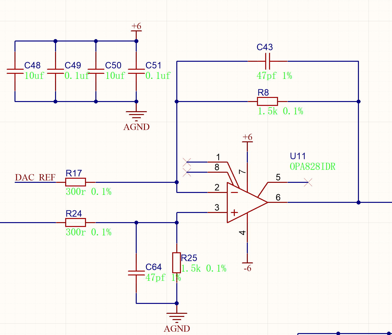
The measured signal first goes through an instrumentation amplifier and is converted to a single-ended signal. It then enters a fixed-gain difference amplifier, which implements:
Vout = 5 × (Vsignal - VDAC_bias)The fixed difference amplifier currently uses a high-speed, low-noise op amp. The resistor values are:
Input resistors: 300 Ω
Feedback / reference-side resistors: 1.5 kΩ
Gain: 5 V/V
After this stage, there is a non-inverting PGA with gain settings:
1 / 2 / 4 / 8
Therefore, the total analog gains are:
5 / 10 / 20 / 40
All noise data below is input-referred RMS noise, calculated after dividing by the corresponding total analog gain.
2. DAC offset circuit
The DAC offset path is used to generate a bipolar offset voltage, so that the DC component of the measured signal can be subtracted before further amplification.
The offset circuit is:
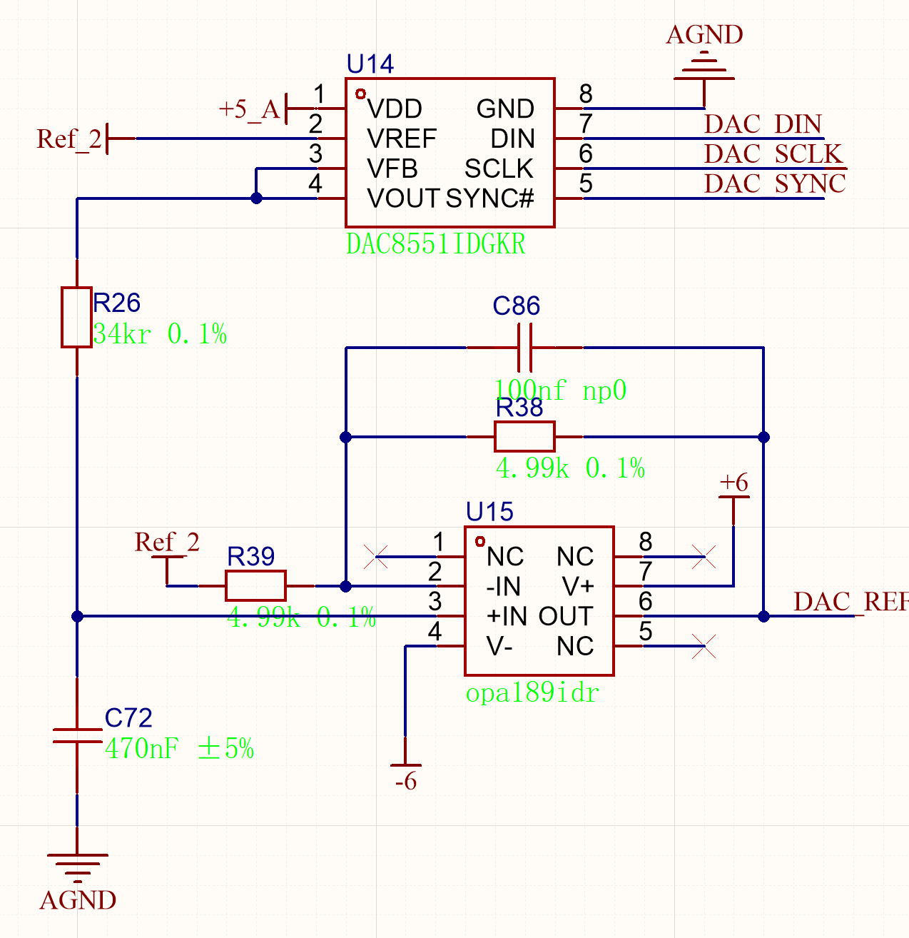
2.048 V precision reference → DAC8551 reference

DAC8551 output → 34 kΩ + 470 nF RC low-pass filter → non-inverting input of offset op amp

2.048 V precision reference → 5 kΩ → inverting input of offset op amp

offset op amp output → 5 kΩ → inverting input of offset op amp
Therefore, the low-frequency transfer function is:
VDAC_bias = 2 × VDAC - 2.048 V
When the DAC output is 1.024 V, the offset amplifier output should be approximately 0 V.
I have tried both OPA189 and OPA828 as the offset amplifier, but the noise level did not change significantly. I also tried different capacitors in parallel with the 5 kΩ feedback resistor, such as 10 nF and 330 pF, but there was no fundamental improvement.
3. Test data
The following data is input-referred RMS noise in volts. Each row corresponds to PGA gain settings:
1 / 2 / 4 / 8
3.1 Full circuit connected
The DAC offset output is connected normally to the fixed 5× difference amplifier.
1 MSPS:
3.95E-05   3.71E-05   3.39E-05   3.18E-05

2 MSPS, average every 2 samples:
3.28E-05   3.20E-05   3.08E-05   2.90E-05
The input-referred noise is around 30–40 µV RMS.
3.2 DAC offset path disconnected
In this test, the DAC offset output is disconnected from the fixed difference amplifier. The original DAC offset input of the difference amplifier is tied directly to AGND. The main signal path is still connected normally.
1 MSPS:
6.46E-06   6.15E-06   4.76E-06   3.92E-06

2 MSPS, average every 2 samples:
4.77E-07   1.46E-06   2.13E-06   2.17E-06
In this condition, the main signal chain can reach a few µV RMS input-referred noise.
3.3 Offset amplifier inputs tied to AGND, but output still connected
In this test:
The non-inverting input of the offset amplifier is tied to AGND.

The 5 kΩ resistor that normally connects the 2.048 V reference to the inverting input is also tied to AGND instead of 2.048 V.

The 5 kΩ feedback resistor remains connected.

The offset amplifier output is still connected to the fixed 5× difference amplifier.
In this condition, the offset amplifier should ideally output 0 V.
However, the measured noise is:
1 MSPS:
3.88E-05   3.94E-05   3.52E-05   3.47E-05

2 MSPS, average every 2 samples:
3.41E-05   3.38E-05   3.31E-05   3.08E-05
This result is almost the same as when the full DAC offset circuit is connected.
Therefore, the noise does not seem to come mainly from the DAC8551 output code itself, nor only from the 2.048 V reference. Even when the offset amplifier inputs are both grounded and the expected output is 0 V, connecting this active 0 V output to the difference amplifier still brings the noise back to the 30–40 µV RMS level.
4. Other tests already performed
To rule out cable effects, I used a shielded cable. The shield is connected to AGND only at the acquisition board side, while the far end of the shield is left floating. The far-end Sense+ and Sense− wires are shorted together.
I also tried removing the cable and shorting Sense+ and Sense− directly at the input connector of the board. As long as the DAC offset amplifier output is connected to the fixed difference amplifier, the noise remains much higher than when the DAC offset path is disconnected.
I also tried splitting the original 300 Ω DAC-bias input resistor of the fixed difference amplifier into:
DAC offset op amp output → 100 Ω → middle node → 200 Ω → difference amplifier inputThen I added a capacitor from the middle node to AGND. However, the noise increased by about 10–20 µV. After removing this capacitor, the noise returned to the original 30–40 µV RMS level.
So this middle-node capacitor did not help. It may have introduced AGND noise or parasitic effects from the temporary wiring.
5. Current thoughts
At this point, I suspect the issue may be related to one or more of the following:
- The DAC offset amplifier output, used as an “active 0 V” or active bias source, is not as quiet as a direct AGND connection.
- The offset amplifier is driving a relatively low input resistance of 300 Ω into the difference amplifier, which may make its output noise, power-supply noise, or stability issues more visible.
- When the active DAC offset source is connected to the difference amplifier, the input network or layout parasitics of the difference amplifier may cause noise peaking.
- The 5 kΩ / 5 kΩ feedback network of the offset amplifier may have too high an impedance, making the inverting node sensitive to parasitic coupling and noise.
6. Planned modification
I am planning to reduce the two 5 kΩ resistors in the DAC offset amplifier to 2.2 kΩ:
Feedback resistor = 2.2 kΩ
Reference input resistor = 2.2 kΩ
Feedback capacitor ≈ 10 nF
This should still keep the same transfer function:
VDAC_bias = 2 × VDAC - 2.048 Vbut with a lower impedance at the inverting node, which may reduce thermal noise and sensitivity to parasitic coupling.
7. Questions
- In this type of circuit, can the noise increase from a few µV RMS to 30–40 µV RMS simply because an active DAC offset source is connected to the difference amplifier?
- Could the 300 Ω DAC-bias input resistor of the difference amplifier be too low for the DAC offset amplifier, causing output noise, supply noise, or stability issues to be injected into the following stage?
- For this kind of structure:
Vout = 5 × (Vsignal - VDAC_bias)should the DAC offset source be designed as a lower-output-impedance and lower-bandwidth precision bias source?
- Is reducing the offset amplifier resistor pair from 5 kΩ / 5 kΩ to 2.2 kΩ / 2.2 kΩ a reasonable direction for reducing noise and parasitic sensitivity?
8. Summary
The main point that confuses me is:
When the DAC offset amplifier inputs are both tied to AGND, its output should ideally be 0 V. However, as soon as this output is connected to the fixed 5× difference amplifier, the system noise becomes almost the same as when the full DAC offset circuit is connected.
Does this behavior look more like a noise / stability problem of the active offset source itself, or more like an issue with the input network / layout of the following difference amplifier?
Thank you.