

Other Parts Discussed in Thread: ADS831
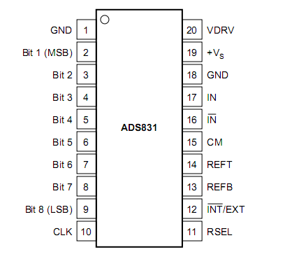
PCB布板时,ads831的模拟地和数字地要不要用0Ω的电阻或磁珠分开。。。我将芯片上的地都直接相连,FPGA产生的CLK给ADS831时,输入给AD的信号会叠加上噪声。我的理解是噪声应该与CLK有关,而CLK边沿的变化影响地,我用示波器观察地,地的噪声变得很大,从而使模拟的信号波形变差。。。。如果要把数字地与模拟地分割,该如何布板,因为ADS831芯片并没有专门的AGND和DGND,只有GND
Other Parts Discussed in Thread: ADS831
PCB布板时,ads831的模拟地和数字地要不要用0Ω的电阻或磁珠分开。。。我将芯片上的地都直接相连,FPGA产生的CLK给ADS831时,输入给AD的信号会叠加上噪声。我的理解是噪声应该与CLK有关,而CLK边沿的变化影响地,我用示波器观察地,地的噪声变得很大,从而使模拟的信号波形变差。。。。如果要把数字地与模拟地分割,该如何布板,因为ADS831芯片并没有专门的AGND和DGND,只有GND