

Other Parts Discussed in Thread: ADS1282

如图,采用的是连续读数模式,电路连接图完全按照如下连接
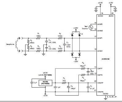
供电DVDD=+3.3V, AVDD/AVSS=±2.5V, VREFP/VREFN=±2.5V,CLK为2.048MHz有源晶振SYNC/nPWDN/nRESET均上拉,未用的M0/M1/MCLK均下拉,
请求指点
Other Parts Discussed in Thread: ADS1282
如图,采用的是连续读数模式,电路连接图完全按照如下连接
供电DVDD=+3.3V, AVDD/AVSS=±2.5V, VREFP/VREFN=±2.5V,CLK为2.048MHz有源晶振SYNC/nPWDN/nRESET均上拉,未用的M0/M1/MCLK均下拉,
请求指点


 这个图片的时序编写命令?