Part Number: LM98725
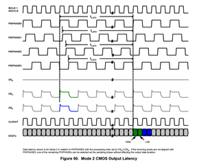
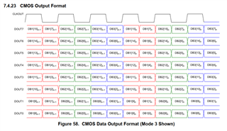
LM98725采用CMOS输出格式时为8bit*2的形式,我这边对接的芯片是8位DVP接口,但是软件上无法实现LM98725时序要求的上下降沿采样高八位,和低八位。仅能实现单种跳变沿的采样。即上升沿采样,或者下降沿采样。
请问是否有什么办法能解决这个问题。
Part Number: LM98725
LM98725采用CMOS输出格式时为8bit*2的形式,我这边对接的芯片是8位DVP接口,但是软件上无法实现LM98725时序要求的上下降沿采样高八位,和低八位。仅能实现单种跳变沿的采样。即上升沿采样,或者下降沿采样。
请问是否有什么办法能解决这个问题。