This thread has been locked.
If you have a related question, please click the "Ask a related question" button in the top right corner. The newly created question will be automatically linked to this question.
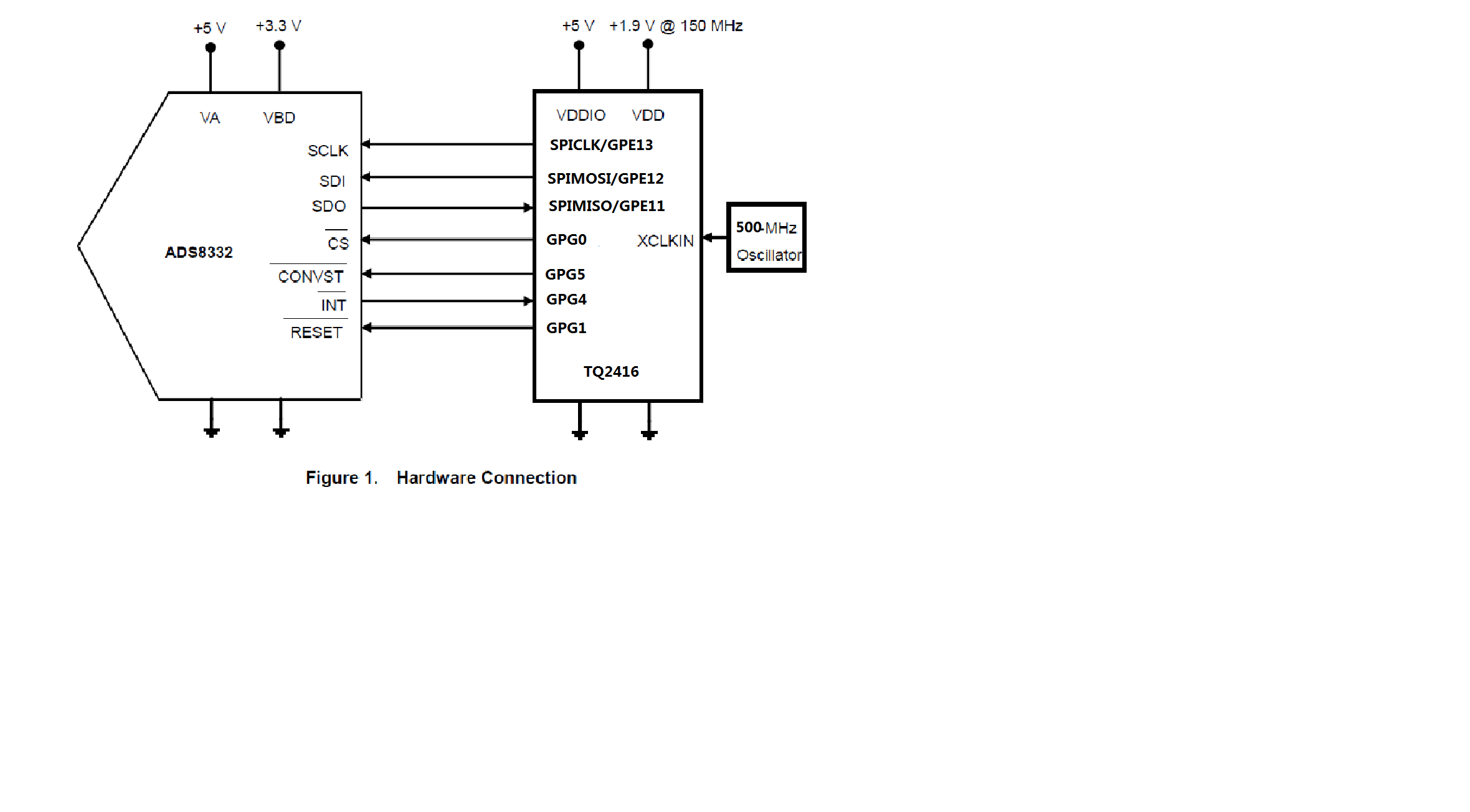
Other Parts Discussed in Thread: ADS8332
ADS8332 + s3c2416
你的问题太泛太大了。难以回答
看到 msp430 + ads8332的定义如下
#define ADS8332_RESET P1.7#define ADS8332_EOC_INT P1.6 #define ADS8332_CDI P1.6#define ADS8332_SCLK P3.7#define ADS8332_CS P3.6#define ADS8332_SDI P3.5#define ADS8332_SDO P3.4 #define ADS8332_CONVST P2.2 #define ADS8332_RESET_1 P1OUT |= ADS8332_RESET#define ADS8332_RESET_0 P1OUT &=~ADS8332_RESET
在arm9 linux 下如何配置呢?
PORT E CONTROL REGISTERS (GPECON, GPEDAT, GPEUDP, GPESEL)
Register Address R/W Description Reset Value
GPECON 0x56000040 R/W Configures the pins of port E 0x0
GPEDAT 0x56000044 R/W The data register for port E 0x0
GPEUDP 0x56000048 R/W Pull-up/down control register for port E 0x55555555
GPESEL 0x5600004c R/W Selects the function of port E 0x0
GPE13 [27:26] 00 = Input 01 = Output
10 = SPICLK0 11 = Reserved
GPE12 [25:24] 00 = Input 01 = Output
10 = SPIMOSI0 11 = Reserved
GPE11 [23:22] 00 = Input 01 = Output
10 = SPIMISO0 11 = Reserved
PORT G CONTROL REGISTERS (GPGCON, GPGDAT, GPGUDP)
If GPG0–GPG7 will be used for wake-up signals from Sleep/Stop/Deep Stop mode, the ports will be set in EINT.
GPGCON 0x56000060 R/W Configures the pins of port G 0x0
GPGDAT 0x56000064 R/W The data register for port G 0x0
GPGUDP 0x56000068 R/W Pull-up/down control register for port G 0x55555555
GPG5 [11:10] 00 = Input 01 = Output
10 = EINT[13] 11 = Reserved
GPG4 [9:8] 00 = Input 01 = Output
10 = EINT[12] 11 = Reserved
GPG3 [7:6] 00 = Input 01 = Output
10 = EINT[11] 11 = Reserved
GPG2 [5:4] 00 = Input 01 = Output
10 = EINT[10] 11 = Reserved
GPG1 [3:2] 00 = Input 01 = Output
10 = EINT[9] 11 = Reserved
GPG0 [1:0] 00 = Input 01 = Output
10 = EINT[8] 11 = Reserved
硬件接线示意图
没发现官网上有相关的ADS8332例程,你可以在社区找找看有没有现成的例程。
我个人觉得这个应该问题需要拿到Processor相关的论坛下进行发帖提问。