This thread has been locked.

If you have a related question, please click the "Ask a related question" button in the top right corner. The newly created question will be automatically linked to this question.

LDC模拟地和数字地 怎么分割和连接

Other Parts Discussed in Thread: ADS1220

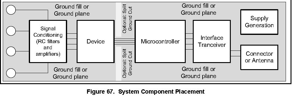
我仔细看了看LDC1000评估板的pcb设计,该设计中将数字地和模拟地分割了,两个地在 
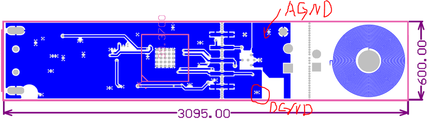
LDC的接地散热片处相连。我发现LDC1000评估板中将数字地连在数字地平面一侧,将模拟地连接在模拟地一侧。但是通常设计中,是将数据转换器的数字地和模拟地都连接在模拟地一侧。请问,ldc1000评估板的这种设计原理是什么?谢谢大家的帮助。

  • 我觉得,数字地和模拟地分开的方式很好啊。

    “但是通常设计中,是将数据转换器的数字地和模拟地都连接在模拟地一侧。”  这不是 TI  的通常设计吧?

  • 原则上是分区不分地。但是如果PCB比较简单或者水平高的情况下,分地是可以取得更好的效果的。

  • 您好,数据转换器的数字地和模拟地在数据转换器的内部都是连接在模拟地上的,很多技术手册上也讲到将这两个地都接在模拟地一侧。可能在具体在使用过程中有一些需要注意的地方吧,如果有这方面的详细的资料就好了。

  • The use of split analog and digital ground planes is not necessary for improved noise performance (although for thermal isolation this option is a worthwhile consideration). However, the use of a solid ground plane or ground fill in PCB areas with no components is essential for optimum performance. If the system being used employs a split digital and analog ground plane, TI generally recommends that the ground planes be connected together as close to the ADS1220 as possible.


    您好,关于“分区不分地”我是这样理解的不知道对不对:分区指的是将模拟电路部分和数字电路部分分开布局;不分地指的是保证地平面的完整性,没有将数字部分和模拟部分下面的地平面分割。   分地,是不是类似图67(ADS1220推荐布局)那样的? 如果分地,数据转换器的模拟地引脚和数字地引脚都是连在模拟地一侧还是两侧都可以,亦或是有其它的连接方法?图67中好像是将模拟地和数字低都连在了模拟地一侧。 如果有数据转换器方面的详细的pcb设计指南就更好了,非常感谢!