This thread has been locked.
If you have a related question, please click the "Ask a related question" button in the top right corner. The newly created question will be automatically linked to this question.
Part Number: ADS1285
您好,我共有两个问题。
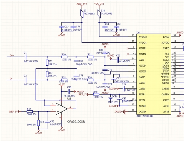
1.如下来,有源正负差分交流信号经IN+ 、IN-,经隔直电容C1、C2后,在偏置到1.25V。经ADC采样。目前发现IN+ 、IN-经隔直电容后会衰减。我怀疑是PGA阻抗不够大,手册没找到具体多大。请问ADS1285内部PGA阻抗多大?
若真的是阻抗太小,能否推荐一个可提供偏置电压的ADC前端低噪声驱动电路。感觉用全差分运放噪声会大。
2.想在咨询下ADS1285内部的Buf,如果读取不及时,可以存几个字节的数据?
您好,PGA输入阻抗大概是22Mohm。ADC的BUF是硬件驱动Modulator,并非存储单元。驱动电路请参见 手册Figure 9-1. Geophone Input Application Example
datasheet
这款芯片官方提供了开发板和对应的设计资料。希望能帮助到您。
https://www.ti.com/tool/ADS1285EVM-PDK