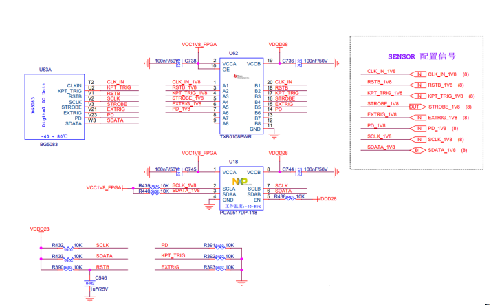
Part Number: TXB0108
The A1 pin of TXB0108PWR chip inputs a 25MHz clock signal normally, but there is no output at the B1 end during testing. Touch the B1 pin with your hand or touch it with an oscilloscope probe, and the B1 pin will output a normal 25MHz clock.
Test conditions:
1、VCCA=1.8V,VCCB=2.8V;
2、OE PIN directly connected to VCCA
The circuit diagram is shown below