This thread has been locked.

If you have a related question, please click the "Ask a related question" button in the top right corner. The newly created question will be automatically linked to this question.

TLIN1028-Q1: LIN SBC can`t wake up from sleep mode by power on

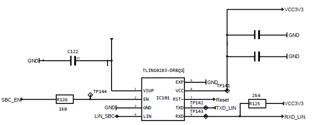
Part Number: TLIN1028-Q1

steps for reproduce the failure:

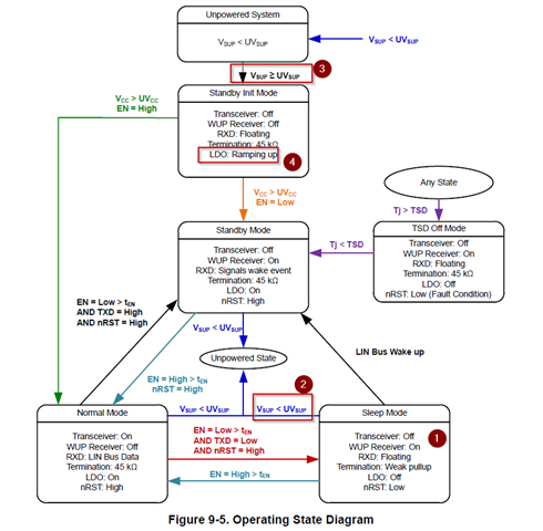
1,configure the system into sleep mode

2,reduce power supply to 0

3,power supply increase again above UVsup

4,the LDO ramping up is not observed as marked in state machine , RST is also keep low.

Question: Could you help explain how this can happen? 

TLIN10283-DRBQ1 used, schematic attached as below

  • 您好,

    已经收到了您的案例,调查需要些时间,感谢您的耐心等待。

  • RST follows Vcc similar to 9.3.7 of the data sheet and would recommend ensuring the VCC3V3 is stable before or with VSUP rising, and EN is high during startup, thanks  

  • sorry, this did NOT resolve my issue.

    in step 1, EN has been pulled low already to put device in sleep mode. It seems the device didn`t enter un-power mode as expected when supply is removed, so how to explain this?   

    additionally, I keep the device ca. 3minutes for step2, then we observed VCC ramping up and RST status change for Step 4, in summary, the device act as its spec, so what capacitor or mechanism keeps the SBC in sleep mode for so long a time not entering un-power mode, this is the confusing point. could you please help? 

  • When you pull EN low to enter sleep mode and then remove VSUP/VCC, the device do not actively pull its internal 3.3 V rail (and its decoupling network) down to 0 V - those caps simply sit there, holding the rail up until they bleed off through leakage. In other words, sleep mode do not equal a built-in discharge circuitry.

    I.e, the external + internal capacitance holds the rail up with at least a 100 nF decoupling cap on VSUP and the recommended (or similar) on the LDO output (VCC3V3).  On top of that, the TLIN1028A-Q1 has on-chip storage capacitances on its LDO output and across its internal regulators. When you pull VSUP to 0 V, none of that capacitance is actively discharged, so VCC3V3 stays above the UVLO threshold (and EN is still low, keeping the part in sleep) until all that charge leaks away, which can easily take minutes if your bulk caps are large.


    Also, un-power mode only occurs once VCC3V3 drops below UV thresholds. See section 7.6 of the data sheet. 
    The device unpowered, high-impedance behavior only kicks in once both VSUP < UVL and the internal VCC3V3 node falls below its own UVLO point. Until then, the internal LDO is still in regulation, so RST stays low and the chip acts as though it is sleeping, not unpowered.

    Only once all the bulk capacitance has bled off through tiny leakage paths (similar to your 3 mins observation) in your decoupling network, board parasitics, and the device itself will VCC3V3 finally dip below its UVLO threshold. At that instant the internal LDO turns off, RST releases high, and on your next VSUP rise you see the full power-on ramp and reset sequence exactly per spec.

    If you want the device to enter its unpowered, high-impedance mode immediately when VSUP is removed, you need to actively discharge its rail capacitance.

    Add a bleed resistor (e.g. 100 k to 1 Mohms) from VCC3V3 to ground. That resistor will drain the LDO output cap quickly enough (time constant RC) so that VCC3V3 falls below UVLO in milliseconds, not minutes.

    Or switch EN and VSUP together, so that as soon as you pull VSUP low you also connect a discharge path on VCC3V3 (via your MCU or an external transistor).

    You can also reduce bulk capacitance if your application allows, use only the minimum decoupling required next to the pin, and locate any large bulk caps off-board or behind a bleed resistor, thanks.