Part Number: DS90UB988-Q1
I'm working with my customer Review DS90UB688 Layout but the Layout design routing problems we have to SWAP OLDI CHO and CH1
The Target will change as below
(1)LVDS EVEN pixel (CH1) of DS90UH688 connected to ODD pixel of TFT LCD Display(2)LVDS ODD pixel(CH0) of DS90UH988 connected to EVEN pixel of TFT LCD Display
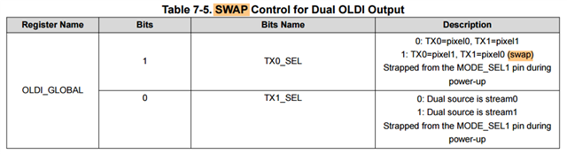
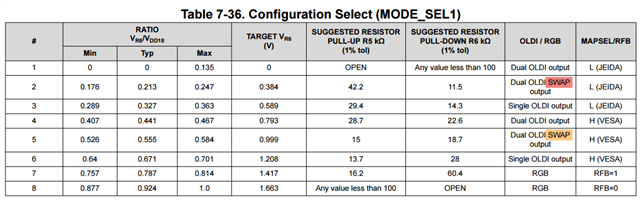
I've see datasheet Table 7-5 we can use TX0_SEL CH0(TX0) and CH1(TX1) can be swapped via register OLDI_GLOBAL[1] setting,and Table 7-36 we can use CH0(TX0) and CH1(TX1) can be swapped via the resistance of VR6 and VDD18 setting.
My question is, the goal of SWAP OLDI CHO and CH1 achieved through software configuring registers, or by changing resistors through hardware, or do both need to be set?