Part Number: SN74LVC1G74
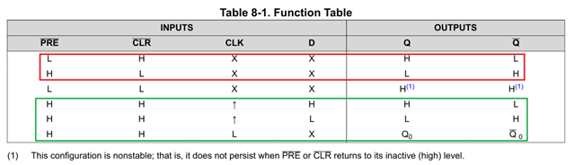
The application circuit of my SN74LVC1G74DCTR latch uses 100K pull-up to 3.3V for D and PRE#, and CLR# is pulled up to 3.3V with a 100nF capacitor to GND. 1. Why does Q sometimes show 0V or around 700mV after power-on? Changing the 100nF to 10nF improves it a bit, but it still happens. 2. Also, what is the output structure of Q and Q# for this device? It seems not to be push-pull.