This thread has been locked.
If you have a related question, please click the "Ask a related question" button in the top right corner. The newly created question will be automatically linked to this question.
想了解下在类似的电路应用中HVD82先上电5V,然后MCU上电(MCU供电可能是3.3V,也可能是5V)。当MCU还没有上电时HVD82的PIN1,PIN2,PIN3,PIN4,分别是什么电平?为啥?
您好,您这样的上电时序是合理的,也就是说先给HVD82上电,然后给MCU上电,相当于HVD82先上电再给输入信号。
如果先给MCU上电,再给HVD82 上电就不合理了。相当于还没上电就给了输入信号了。
那您的问题是,给HVD82上电,但此时没有输入信号, 输入引脚2,3,4的逻辑状态应该是不确定的,但是HVD82 有receiver failsafe保护电路,当driver idle时候,输出也应该是个failsafe的逻辑高电平。
三种失效条件:
• open bus conditions such as a disconnected connector
• shorted bus conditions such as cable damage shorting the twisted-pair together, or
• idle bus conditions that occur when no driver on the bus is actively driving
In any of these cases, the differential receiver will output a failsafe logic High state so that the output of the receiver is not indeterminate.
谢谢你的回答。
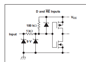
但是在之前那个过程中,我测试发现,如4脚电平是1/2VCC左右,而内部框图显示是上拉到VCC的,这个该怎么理解呢?


 想了解下在类似的电路应用中HVD82先上电5V,然后MCU上电(MCU供电可能是3.3V,也可能是5V)。当MCU还没有上电时HVD82的PIN1,PIN2,PIN3,PIN4,分别是什么电平?为啥?