

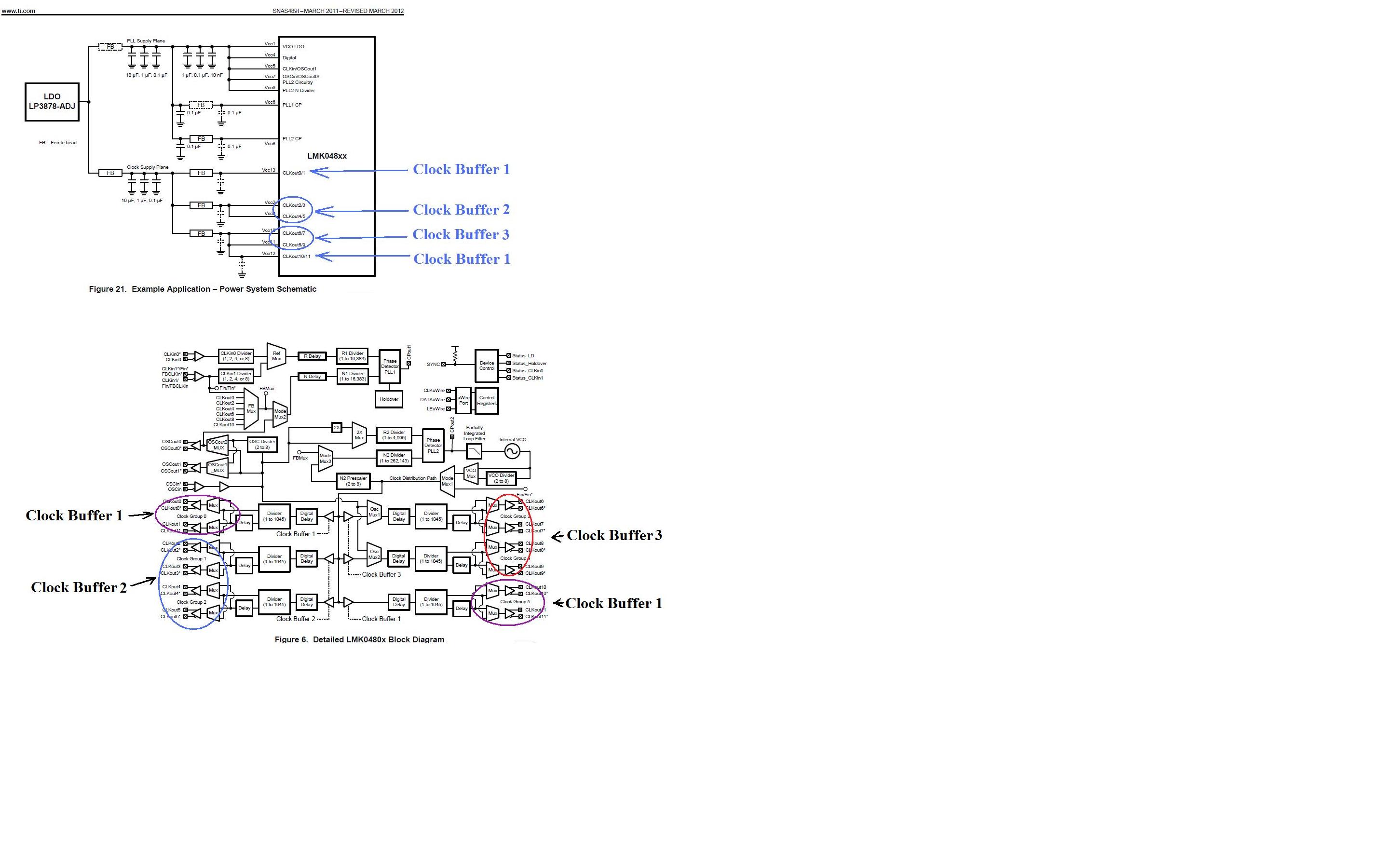
DATASHEET里的FIGURE 2( Example Application - Power System Schematic ),Clockout的供电分组是:
( Clock0/1 )、( Clock2/3+Clock4/5 )、( Clock6/7+Clock8/9+Clock10/11 )。
可是按照Figure 6(Detailed LMK0480x Block Diagram ),Clock Buffer 的分组是:
( Clock0/1+Clock10/11 )、( Clock2/3+Clock4/5 )、( Clock6/7+Clock8/9 )。
上述( FIGURE 2 与 Figure 6 )哪个正确呢?
