This thread has been locked.
If you have a related question, please click the "Ask a related question" button in the top right corner. The newly created question will be automatically linked to this question.
Part Number: SN65176B
SN65176BDR TI专家 你好 我想请问下 这个芯片1脚(RO)内部电路是怎么处理的,5V-VCC供电 ,但在RO脚输出上拉了3.3V,输出高电平时是5V 还是3.3V ?
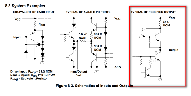
您好,参考数据手册P15的内部架构,Pin1即为接收器的输出端,根据它的内部架构可以看出,上面FET导通的时候,下面闭合,R=H,反之,当下面导通,上面闭合的时候,R=L。这个引脚不需要外部上拉。https://www.ti.com.cn/lit/ds/symlink/sn65176b.pdf