This thread has been locked.
If you have a related question, please click the "Ask a related question" button in the top right corner. The newly created question will be automatically linked to this question.
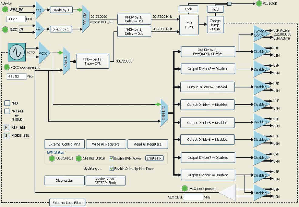
I read paper "CDCE72010 Phase Noise Performance and Jitter Cleaning Ability" and use "Passive Loop Filter Circuit" and "CDCE72010 Device Configuration" on this paper, calculate them with "CDCE72010_PLL_Calculation_V1.08.xls",then I find the "phase margin" and "gain peaking" of the filter is not satisfied.Can you explain it for me? Thanks!
Hi Shuai,
as for peaking and margin issues, please optimize PLL loop parameters to match your need. The link www.ti.com.cn/.../zhca079.pdf is one paper on how to optimize loop design for your reference. Please let me know your concern if you have. thanks.
regards,
Steven