This thread has been locked.

If you have a related question, please click the "Ask a related question" button in the top right corner. The newly created question will be automatically linked to this question.

DS90UH941AS-Q1: 如何生成941AS+928Q的Pattern初始化参数表以及上电时序控制

Part Number: DS90UH941AS-Q1
Other Parts Discussed in Thread: ALP, USB2ANY

应用场景:

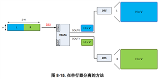
在使用一路MIPI DSI4lane 输入2560x768拼接RGB888 数据到 DS90UH941AS-Q1经过内部分离器分成两路1280x768的串行信号分别输入2路DS90UB928Q进行解串后转换为LVDS信号,分别输出道两块LVDS Panel。

如规格书下图所示,

1、MIPI DSI 两路1280x768左右拼接未完成情况下 941AS的Pattern发生器是否可以生成两路1280x768 串行信号输出供调试屏幕使用?

2、941AS以及928Q的初始化参数是否有工具可以生成符合上电时序要求顺序的初始化参数列表?

3、是否需要先通过2:2单路Pattern来点亮LVDS 屏幕,941AS以及928Q的初始化参数改如何配置

  • 您好,

    为更加有效地解决您的问题,我已将您的问题发布在E2E英文技术论坛上,请更了解这款芯片的TI资深工程师为您解答,一旦得到回复后我会立即回复给您。帖子链接如下,您也可以关注帖子,以方便查看或追问后续疑问。

    英文论坛对应子论坛链接:

    https://e2e.ti.com/support/interface-group/interface/f/interface-forum/1188237/ds90uh941as-q1-pattern-initialization-parameters-for-941as-928q-and-power-up-timing-control

  • 您好,得到E2E英文技术论坛工程师如下回复:

    1.) The 941AS does come with two different PatGen blocks, so you should be able to generate two different patterns. Is ALP being used? If ALP is being used, the pattern generator section under the 941AS Profile should have a PatGen Select option at the bottom. Using this, you should be able to tab between the two different patterns being sent out and verify whether the output and screens work.

    2&3.) What do you mean by initialization parameters? Do you mean enabling splitter mode, PatGen, and register values at start up? Or do you mean ensuring the correct power-up timings during the power up sequence to make sure the device functions? 

    Additionally, could you possibly provide more information regarding the customers setup? Such as the Active Video Resolutions, the PCLK rate and the DSI clock rate, and the DSI mode being used? I would appreciate it!

    我尝试翻译如下:

    1、941AS确实随附了两个不同的PatGen模块,因此您应该能够生成两个不同的模式。是否使用ALP?如果正在使用ALP,941AS Profile 文件下的pattern generator 部分的底部应该有PatGen Select选项。使用此选项,您应该能够在发出的两种不同模式之间进行切换,并验证输出和屏幕是否正常工作。

    2和3、)初始化参数是什么意思?您的意思是在启动时启用splitter 模式,PatGen和寄存器值吗?或者,您是要确保在通电过程中正确的上电时序以确保设备正常工作?

    此外,您能否提供有关设置的更多信息?例如Active Video分辨率,PCLK速率和DSI时钟速率以及正在使用的DSI模式?非常感谢!

  • 感谢回复,

    2)3)初始化参数是指 941AS/928Q 输出测试模式Pattern的寄存器配置,如果可以,先帮忙给出下面参数One Port DSI Input,One Port al FPD-Link III Output的Pattern 寄存器配置,Pattern使用ColorBar或着红/蓝/绿纯色。 

    m_wHactive = 1280;

    m_wHpw = 36;
    m_wHbp = 160;
    m_wHfp = 174;
    m_wVactive = 768;
    m_wVpw = 4;
    m_wVbp = 24;
    m_wVfp = 24;
    m_wFps = 60;
    MIPI DSI :4Lane,RGB888, SYNC PULSE Mode
    MIPICLK = 244MHz, PCLK = 81MHz
    上电时序已在941AS DataSheet找到说明,目前使用参考B的时序方式,SOC MIPI 已正常输出后再初始化941AS/928Q
  • 关于Pattern Generation,请看下下面文档是否有帮助:

    https://www.ti.com/lit/an/snla132g/snla132g.pdf

    也有对应的中文版本:https://www.ti.com.cn/cn/lit/an/zhcaag6g/zhcaag6g.pdf

  • 这篇文档有详细说明了Pattern寄存器的使用方法,参考文档说明设定928Q的Pattern寄存器相关参数如下:但是Panel没有任何显示,时序符合Panel的要求,全部使用928Q内部CLK,请帮忙确认0x64/0x65/0x39寄存器设定是否正确,除一下寄存器外是否有其他寄存器还需要设定,如0x01中的Reset控制等?

        //Internal CLK DIV
        I2C_Write(0x2C,0x66,0x03,I2C_FMT_A8D8); //Addr
        I2C_Write(0x2C,0x67,0x03,I2C_FMT_A8D8); //Data

        //HActive LSB
        I2C_Write(0x2C,0x66,0x07,I2C_FMT_A8D8); //Addr
        I2C_Write(0x2C,0x67,0x00,I2C_FMT_A8D8); //Data

        //HActive MSB& VActive LSB
        I2C_Write(0x2C,0x66,0x08,I2C_FMT_A8D8); //Addr
        I2C_Write(0x2C,0x67,0x05,I2C_FMT_A8D8); //Data
        //VActive MSB
        I2C_Write(0x2C,0x66,0x09,I2C_FMT_A8D8); //Addr
        I2C_Write(0x2C,0x67,0x30,I2C_FMT_A8D8); //Data

        //HTotal LSB
        I2C_Write(0x2C,0x66,0x04,I2C_FMT_A8D8); //Addr
        I2C_Write(0x2C,0x67,0x72,I2C_FMT_A8D8); //Data
        //HTotal MSB& VTotal LSB
        I2C_Write(0x2C,0x66,0x05,I2C_FMT_A8D8); //Addr
        I2C_Write(0x2C,0x67,0x26,I2C_FMT_A8D8); //Data
        //VTotal MSB
        I2C_Write(0x2C,0x66,0x06,I2C_FMT_A8D8); //Addr
        I2C_Write(0x2C,0x67,0x33,I2C_FMT_A8D8); //Data

        //HBP
        I2C_Write(0x2C,0x66,0x0C,I2C_FMT_A8D8); //Addr
        I2C_Write(0x2C,0x67,0xA0,I2C_FMT_A8D8); //Data
        //VBP
        I2C_Write(0x2C,0x66,0x0D,I2C_FMT_A8D8); //Addr
        I2C_Write(0x2C,0x67,0x18,I2C_FMT_A8D8); //Data

        //HSW
        I2C_Write(0x2C,0x66,0x0A,I2C_FMT_A8D8); //Addr
        I2C_Write(0x2C,0x67,0x24,I2C_FMT_A8D8); //Data
        //VSW
        I2C_Write(0x2C,0x66,0x0B,I2C_FMT_A8D8); //Addr
        I2C_Write(0x2C,0x67,0x04,I2C_FMT_A8D8); //Data

        //POL&HV_DIS
        I2C_Write(0x2C,0x66,0x0E,I2C_FMT_A8D8); //Addr
        I2C_Write(0x2C,0x67,0x00,I2C_FMT_A8D8); //Data

        //FPS
        I2C_Write(0x2C,0x66,0x0F,I2C_FMT_A8D8); //Addr
        I2C_Write(0x2C,0x67,0x18,I2C_FMT_A8D8); //Data

        I2C_Write(0x2C,0x65,0x03,I2C_FMT_A8D8); //
        I2C_Write(0x2C,0x39,0x02,I2C_FMT_A8D8); //
        I2C_Write(0x2C,0x64,0x51,I2C_FMT_A8D8); //
    已确认Panel硬件连接正常,使用Panel自己的自测模式屏幕可以输出各种Pattern, 使用928Q送给Panel的Pattern信号测试无任何画面输出。
    PASS PIN 低电平,LOCK PIN高电平
  • 新年快乐!

    我已将上述问题反馈给 E2E 工程师,请耐心等待他们的解答!得到答复后,我也会回复到这里。

  • Dear Amy,

    看英文帖子还没有回复哦,帮忙追一下可以吗?

    有确认928Q的VDD33/VDDIO等供电都有3.3V,RTERM = 100Q ,请帮忙确认以下PIN脚设计是否有正确,MODE_SEL 对应R4=1.354V R6=2.046V,是否存在问题?

    基于我当前产品的使用场景:每个928Q只点一块LVDS Panel,且没有Audio传输需求,MODE_SEL应该配置为下面哪组配置?

    完全照搬Pattern使用说明中这一组初始化参数,只是修改对应内部200M为160M计算PCLK(928Q内置时钟源为160M),其他都按下面截图中参数设定,不接LVDS屏幕,测量LVDS输出,LVDS CLK/DATA  Lane均只有高低电平变化,没有LVDS信号波形出来,

       //Internal CLK DIV
        I2C_Write(0x2C,0x66,0x03,I2C_FMT_A8D8); //Addr
        I2C_Write(0x2C,0x67,0x05,I2C_FMT_A8D8); //Data

        //HActive LSB
        I2C_Write(0x2C,0x66,0x07,I2C_FMT_A8D8); //Addr
        I2C_Write(0x2C,0x67,0x20,I2C_FMT_A8D8); //Data

        //HActive MSB& VActive LSB
        I2C_Write(0x2C,0x66,0x08,I2C_FMT_A8D8); //Addr
        I2C_Write(0x2C,0x67,0x03,I2C_FMT_A8D8); //Data
        //VActive MSB
        I2C_Write(0x2C,0x66,0x09,I2C_FMT_A8D8); //Addr
        I2C_Write(0x2C,0x67,0x1E,I2C_FMT_A8D8); //Data

        //HTotal LSB
        I2C_Write(0x2C,0x66,0x04,I2C_FMT_A8D8); //Addr
        I2C_Write(0x2C,0x67,0x98,I2C_FMT_A8D8); //Data
        //HTotal MSB& VTotal LSB
        I2C_Write(0x2C,0x66,0x05,I2C_FMT_A8D8); //Addr
        I2C_Write(0x2C,0x67,0xD4,I2C_FMT_A8D8); //Data
        //VTotal MSB
        I2C_Write(0x2C,0x66,0x06,I2C_FMT_A8D8); //Addr
        I2C_Write(0x2C,0x67,0x20,I2C_FMT_A8D8); //Data

        //HBP
        I2C_Write(0x2C,0x66,0x0C,I2C_FMT_A8D8); //Addr
        I2C_Write(0x2C,0x67,0xD8,I2C_FMT_A8D8); //Data
        //VBP
        I2C_Write(0x2C,0x66,0x0D,I2C_FMT_A8D8); //Addr
        I2C_Write(0x2C,0x67,0x23,I2C_FMT_A8D8); //Data

        //HSW
        I2C_Write(0x2C,0x66,0x0A,I2C_FMT_A8D8); //Addr
        I2C_Write(0x2C,0x67,0x0A,I2C_FMT_A8D8); //Data
        //VSW
        I2C_Write(0x2C,0x66,0x0B,I2C_FMT_A8D8); //Addr
        I2C_Write(0x2C,0x67,0x02,I2C_FMT_A8D8); //Data

        //POL&HV_DIS
        I2C_Write(0x2C,0x66,0x0E,I2C_FMT_A8D8); //Addr
        I2C_Write(0x2C,0x67,0x03,I2C_FMT_A8D8); //Data

        I2C_Write(0x2C,0x65,0x03,I2C_FMT_A8D8); //
        I2C_Write(0x2C,0x39,0x02,I2C_FMT_A8D8); //
        I2C_Write(0x2C,0x64,0x11,I2C_FMT_A8D8); //
  • 您好,由于时差原因,美国的工程师明天应该会跟进。我已将上述问题咨询美国工程师了。

  • 感谢,

    1、USB2ANY 是只有EVM才能使用的调试板还是有单独转接板可以连接PC和RealBoard使用?

    2、很多文档提到的AN-2198文档是指哪份文档,帮忙贴一下链接

  • 1、USB2ANY 是单独转接板可以连接PC和RealBoard使用,见下面USB2ANY 用户指南:

    https://www.ti.com.cn/cn/lit/ug/snau228/snau228.pdf

    2、就是上面已经贴出来的链接:

    https://www.ti.com/lit/an/snla132g/snla132g.pdf

    很高兴看到您已经在E2E英文技术论坛上做出了回复,由于时差问题他们一般是晚上回帖,您可以关注帖子及时查看回复。

  • Dear Amy,

    USB2ANY 转接板有购买或申请渠道可以提供吗,对调试解决问题帮助是否有直接帮助?

  • 您在E2E英文论坛的问题已得到回复:

    First, is the 928Q being written and read locally, or are they being read remotely via the 941AS?

    Next, double check that all the registers being written to are in fact changing their values, as well as reading the 0x00 register to see what the device ID is.

    Also, if you could also supply the 941AS schematic, I would appreciate it. I will continue looking at the 928 schematic, but so far I have not seen any issues.

    One thing I am worried about is the device IDs. Please make sure that each serializer and deserializer has a unique ID assigned to them via the IDx pin. Having multiple devices with the same ID may cause issues with reading and writing to registers.

    From what I can tell in the commands, it does seem like they should be having an effect on the outputs, so its strange that they are not. I will look into whether we have seen anything like this before.

  • Hi Gene,

    如果您的问题还未解决,请跟进E2E英文论坛:https://e2e.ti.com/support/interface-group/interface/f/interface-forum/1188237/ds90uh941as-q1-pattern-initialization-parameters-for-941as-928q-and-power-up-timing-control

    Did you also check the hardware of both 928s?

    Yes, the value of the STS register should be 0x28. On the 941AS, the RX_INT bit of the STS register is used to indicate when the INTB_IN pin of the attached deserializer is active, it does not need to be to be active for functionality.

    One thing I noticed after looking at the value of the TX_MODE_STS register value, it reads out 8B, even though when looking at the schematic, it should read out as 8F. I just want to confirm, did you adjust the resistors for MODE_SEL0 to disable splitter mode on the 941AS?

    For MODE_SEL1, which setting is being used on the 941AS? Is CLOCK enabled or disabled?

    Do you still have your friends 947 and 928 boards? If so, could you compare these same registers and see if the STS and GENERAL_STS see the link and indicate it via their register bits?

    Is the schematic of the good 928Q board similar? would it be possible to send it?