This thread has been locked.
If you have a related question, please click the "Ask a related question" button in the top right corner. The newly created question will be automatically linked to this question.
Part Number: DP83TC812R-Q1
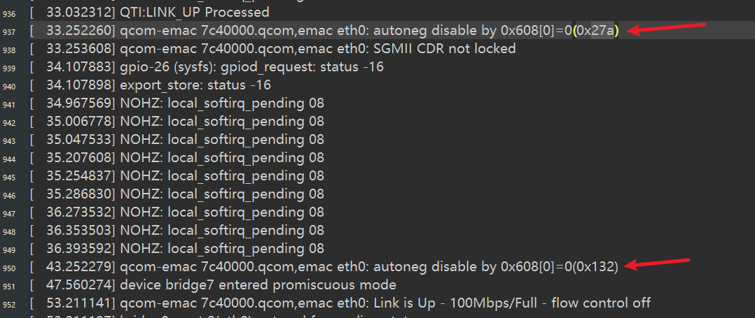
已知DP83TC812的608寄存器在值等于0x27a时phy通信正常,但偶发值会突变成0x132,我想知道为何会发生这个变化应该怎么避免这种变化?
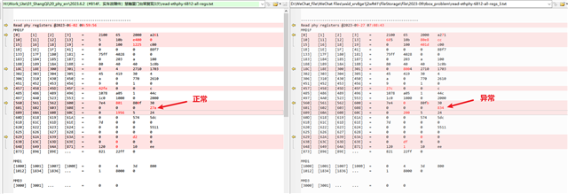
您好,0x608的寄存器变化来看,像是serdes 的RX数据的顺序发生了变化,导致bit8这里SGMII RX bus invert polarity极性出现相反。
看下这里的配置bit15-14是不是也发生了变化。
4A0这个寄存器倒是没什么变化
将 608 寄存器值改为 27a 后,恢复正常;
您好,从寄存器值的改变来看,就是bit8这里的SGMII极性的交换,而DP83TC812不支持自动极性交换。所以我想是不是这里的原因导致。
0x60A寄存器可以说明SGMII的link状态,当608的值改变之后,看下0x60A的bit 11的SGMII link是否down掉。
什么情况下会导致这个问题:bit8这里的SGMII极性的交换呢?
您好,这个问题应该是和SGMII协议标准有关,具体要看下协议标准。
我想DP83TC812传输的数据格式应该是遵循协议的,并且不支持自动极性交换。 而和MAC相连的MDI接口是不是自适应极性交换的,所以当传输的数据极性发生改变的时候,DP83TC812侧会报错。
但是这是一个偶发的事件,如果MDI接口出现极性相反了,应该会变成一个必现的
您好,偶发的事件只发生在一片芯片上还是多片?我帮您确认下。
多片,而且应该在忙的时候比较多出现,但我还是不太明白你说什么情况导致mdl极性反转sgmll极性反转,程序主动改变sgmll极性,最后导致link失败?
如果你是Ti公司研发支持,我感觉可以电话沟通:13950168929,我电话,如果你那边不方便的话那也没关系的
您好,抱歉我们目前的支持方式是以论坛的形式沟通的。
我刚已经把您的问题升级到英文E2E上了,请关注美国工程师的回复:
https://e2e.ti.com/support/interface-group/interface/f/interface-forum/1286014/dp83tc812r-q1-0x608-has-changed-from-0x27a-to-0x132
有任何问题,可直接跟进。
好的,谢谢你了
您好,E2E给出回复了,应该是driver的bug,并且给了配置例程,您试试是否可以解决您的问题。
// SPDX-License-Identifier: GPL-2.0
/*
 * Driver for the Texas Instruments DP83TC812 PHY
 *
 * Copyright (C) 2021 Texas Instruments Incorporated - http://www.ti.com/
 *
 */

#include <linux/ethtool.h>
#include <linux/etherdevice.h>
#include <linux/kernel.h>
#include <linux/mii.h>
#include <linux/module.h>
#include <linux/of.h>
#include <linux/phy.h>
#include <linux/netdevice.h>

#define DP83TC812_CS1_0_PHY_ID	0x2000a270
#define DP83TC812_CS2_0_PHY_ID	0x2000a271
#define DP83TC813_CS2_0_PHY_ID	0x2000a211
#define DP83TC814_CS2_0_PHY_ID	0x2000a261

#define DP83812_DEVADDR		0x1f
#define DP83812_DEVADDR_MMD1	0x1

#define DP83812_STRAP		0x45d
#define MII_DP83812_SGMII_CTRL	0x608
#define SGMII_CONFIG_VAL	0x027B
#define MII_DP83812_RGMII_CTRL	0x600
#define MII_DP83812_INT_STAT1	0x12
#define MII_DP83812_INT_STAT2	0x13
#define MII_DP83812_INT_STAT3	0x18
#define MII_DP83812_RESET_CTRL	0x1f

#define DP83812_HW_RESET	BIT(15)
#define DP83812_SW_RESET	BIT(14)

/* INT_STAT1 bits */
#define DP83812_RX_ERR_CNT_HALF_FULL_INT_EN	BIT(0)
#define DP83812_TX_ERR_CNT_HALF_FULL_INT_EN	BIT(1)
#define DP83812_MS_TRAIN_DONE_INT_EN		BIT(2)
#define DP83812_ESD_EVENT_INT_EN		BIT(3)
#define DP83812_LINK_STAT_INT_EN		BIT(5)
#define DP83812_ENERGY_DET_INT_EN		BIT(6)
#define DP83812_LINK_QUAL_INT_EN		BIT(7)

/* INT_STAT2 bits */
#define DP83812_JABBER_INT_EN		BIT(0)
#define DP83812_POL_INT_EN		BIT(1)
#define DP83812_SLEEP_MODE_INT_EN	BIT(2)
#define DP83812_OVERTEMP_INT_EN		BIT(3)
#define DP83812_FIFO_INT_EN		BIT(4)
#define DP83812_PAGE_RXD_INT_EN		BIT(5)
#define DP83812_OVERVOLTAGE_INT_EN	BIT(6)
#define DP83812_UNDERVOLTAGE_INT_EN	BIT(7)

/* INT_STAT3 bits */
#define DP83812_LPS_INT_EN		BIT(0)
#define DP83812_WUP_INT_EN		BIT(1)
#define DP83812_WAKE_REQ_INT_EN		BIT(2)
#define DP83811_NO_FRAME_INT_EN		BIT(3)
#define DP83811_POR_DONE_INT_EN		BIT(4)
#define DP83812_SLEEP_FAIL_INT_EN	BIT(5)

/* RGMII_CTRL bits */
#define DP83812_RGMII_EN		BIT(3)

/* SGMII CTRL bits */
#define DP83812_SGMII_AUTO_NEG_EN	BIT(0)
#define DP83812_SGMII_EN		BIT(9)

/* Strap bits */
#define DP83812_MASTER_MODE	BIT(9)
#define DP83812_RGMII_IS_EN	BIT(7)

/* RGMII ID CTRL */
#define DP83812_RGMII_ID_CTRL	0x602
#define DP83812_RX_CLK_SHIFT	BIT(1)
#define DP83812_TX_CLK_SHIFT	BIT(0)

enum dp83812_chip_type {
	DP83812_CS1 = 0,
	DP83812_CS2,
	DP83813_CS2,
	DP83814_CS2,
};

struct dp83812_init_reg {
	int	reg;
	int	val;
};

static const struct dp83812_init_reg dp83812_master_cs1_0_init[] = {
	{0x523, 0x0001},
	{0x800, 0xf864},
	{0x803, 0x1552},
	{0x804, 0x1a66},
	{0x805, 0x1f7b},
	{0x81f, 0x2a88},
	{0x825, 0x40e5},
	{0x82b, 0x7f3f},
	{0x830, 0x0543},
	{0x836, 0x5008},
	{0x83a, 0x08e0},
	{0x83b, 0x0845},
	{0x83e, 0x0445},
	{0x855, 0x9b9a},
	{0x85f, 0x2010},
	{0x860, 0x6040},
	{0x86c, 0x1333},
	{0x86b, 0x3e10},
	{0x872, 0x88c0},
	{0x873, 0x0003},
	{0x879, 0x000f},
	{0x87b, 0x0070},
	{0x87c, 0x003f},
	{0x89e, 0x00aa},
	{0x523, 0x0000},
};

static const struct dp83812_init_reg dp83812_master_cs2_0_init[] = {
	{0x523, 0x0001},
	{0x81C, 0x0fe2},
	{0x872, 0x0300},
	{0x879, 0x0f00},
	{0x806, 0x2952},
	{0x807, 0x3361},
	{0x808, 0x3D7B},
	{0x83E, 0x045F},
	{0x834, 0x8000},
	{0x862, 0x00E8},
	{0x896, 0x32CB},
	{0x03E, 0x0009},
	{0x01f, 0x4000},
	{0x523, 0x0000},
};

static const struct dp83812_init_reg dp83812_slave_cs1_0_init[] = {
	{0x523, 0x0001},
	{0x803, 0x1b52},
	{0x804, 0x216c},
	{0x805, 0x277b},
	{0x827, 0x3000},
	{0x830, 0x0543},
	{0x83a, 0x0020},
	{0x83c, 0x0001},
	{0x855, 0x9b9a},
	{0x85f, 0x2010},
	{0x860, 0x6040},
	{0x86c, 0x0333},
	{0x872, 0x88c0},
	{0x873, 0x0021},
	{0x879, 0x000f},
	{0x87b, 0x0070},
	{0x87c, 0x0002},
	{0x897, 0x003f},
	{0x89e, 0x00a2},
	{0x510, 0x000f},
	{0x523, 0x0000},
};

static const struct dp83812_init_reg dp83812_slave_cs2_0_init[] = {
	{0x523, 0x0001},
	{0x873, 0x0821},
	{0x896, 0x22ff},
	{0x89E, 0x0000},
	{0x01f, 0x4000},
	{0x523, 0x0000},
};

struct dp83812_private {
	int chip;
	bool is_master;
	bool is_rgmii;
	bool is_sgmii;
};

static int dp83812_read_straps(struct phy_device *phydev)
{
	struct dp83812_private *dp83812 = phydev->priv;
	int strap;

	strap = phy_read_mmd(phydev, DP83812_DEVADDR, DP83812_STRAP);
	if (strap < 0)
		return strap;

	printk("%s: Strap is 0x%X\n", __func__, strap);
	if (strap & DP83812_MASTER_MODE)
		dp83812->is_master = true;

	if (strap & DP83812_RGMII_IS_EN)
		dp83812->is_rgmii = true;
	return 0;
};

static int dp83812_reset(struct phy_device *phydev, bool hw_reset)
{
	int ret;

	if (hw_reset)
		ret = phy_write_mmd(phydev, DP83812_DEVADDR, MII_DP83812_RESET_CTRL,
				DP83812_HW_RESET);
	else
		ret = phy_write_mmd(phydev, DP83812_DEVADDR, MII_DP83812_RESET_CTRL,
				DP83812_SW_RESET);

	if (ret)
		return ret;

	mdelay(100);

	return 0;
}

static int dp83812_phy_reset(struct phy_device *phydev)
{
	int err;
	int ret;

	err = phy_write_mmd(phydev, DP83812_DEVADDR, MII_DP83812_RESET_CTRL, DP83812_HW_RESET);
	if (err < 0)
		return err;

	ret = dp83812_read_straps(phydev);
	if (ret)
		return ret;

	return 0;
}

static int dp83812_write_seq(struct phy_device *phydev, const struct
				dp83812_init_reg *init_data, int size)
{
	int ret;
	int i;

	for (i = 0; i < size; i++) {
		ret = phy_write_mmd(phydev, DP83812_DEVADDR, init_data[i].reg,
					init_data[i].val);
	if (ret)
		return ret;
	}
	return 0;
}

static int dp83812_chip_init(struct phy_device *phydev)
{
	struct dp83812_private *dp83812 = phydev->priv;
	int ret;

	ret = dp83812_reset(phydev, true);
	if (ret)
		return ret;

	phydev->autoneg = AUTONEG_DISABLE;
	phydev->speed = SPEED_100;
	phydev->duplex = DUPLEX_FULL;
	linkmode_set_bit(ETHTOOL_LINK_MODE_100baseT_Full_BIT,
		 phydev->supported);

	if (dp83812->is_master)
		ret = phy_write_mmd(phydev, DP83812_DEVADDR_MMD1, 0x0834, 0xc001);
		// ret = phy_write_mmd(phydev, DP83812_DEVADDR, 0x0834, 0xc001);
	else
		ret = phy_write_mmd(phydev, DP83812_DEVADDR_MMD1, 0x0834, 0x8001);
		// ret = phy_write_mmd(phydev, DP83812_DEVADDR, 0x0834, 0x8001);

	switch (dp83812->chip) {
	case DP83812_CS1:
		if (dp83812->is_master)
			ret = dp83812_write_seq(phydev,
						dp83812_master_cs1_0_init,
						ARRAY_SIZE(dp83812_master_cs1_0_init));
		else
			ret = dp83812_write_seq(phydev,
						dp83812_slave_cs1_0_init,
						ARRAY_SIZE(dp83812_slave_cs1_0_init));
	break;
	case DP83812_CS2:
		if (dp83812->is_master)
			ret = dp83812_write_seq(phydev,
						dp83812_master_cs2_0_init,
						ARRAY_SIZE(dp83812_master_cs2_0_init));
		else
			ret = dp83812_write_seq(phydev,
						dp83812_slave_cs2_0_init,
						ARRAY_SIZE(dp83812_slave_cs2_0_init));
	break;
	case DP83813_CS2:
		if (dp83812->is_master)
			ret = dp83812_write_seq(phydev,
						dp83812_master_cs2_0_init,
						ARRAY_SIZE(dp83812_master_cs2_0_init));
		else
			ret = dp83812_write_seq(phydev,
						dp83812_slave_cs2_0_init,
						ARRAY_SIZE(dp83812_slave_cs2_0_init));
	break;
	case DP83814_CS2:
		if (dp83812->is_master)
			ret = dp83812_write_seq(phydev,
						dp83812_master_cs2_0_init,
						ARRAY_SIZE(dp83812_master_cs2_0_init));
		else
			ret = dp83812_write_seq(phydev,
						dp83812_slave_cs2_0_init,
						ARRAY_SIZE(dp83812_slave_cs2_0_init));
	break;
	default:
		return -EINVAL;
	};

	if (ret)
		return ret;

	mdelay(10);
	// phy_write_mmd(phydev, DP83812_DEVADDR, 0x523, 0x00);
	/* Do a soft reset to restart the PHY with updated values */
	return dp83812_reset(phydev, false);
}

static int dp83812_config_init(struct phy_device *phydev)
{
	struct device *dev = &phydev->mdio.dev;
	s32 rx_int_delay;
	s32 tx_int_delay;
	int rgmii_delay;
	int value, ret;

	ret = dp83812_chip_init(phydev);
	if (ret)
		return ret;

	if (phy_interface_is_rgmii(phydev)) {
		rx_int_delay = phy_get_internal_delay(phydev, dev, NULL, 0,
						      true);

		if (rx_int_delay <= 0)
			rgmii_delay = 0;
		else
			rgmii_delay = DP83812_RX_CLK_SHIFT;

		tx_int_delay = phy_get_internal_delay(phydev, dev, NULL, 0,
						      false);
		if (tx_int_delay <= 0)
			rgmii_delay &= ~DP83812_TX_CLK_SHIFT;
		else
			rgmii_delay |= DP83812_TX_CLK_SHIFT;

		if (rgmii_delay) {
			ret = phy_set_bits_mmd(phydev, DP83812_DEVADDR_MMD1,
					       DP83812_RGMII_ID_CTRL,
					       rgmii_delay);
			if (ret)
				return ret;
		}
	}

	if (phydev->interface == PHY_INTERFACE_MODE_SGMII) {
		value = phy_read(phydev, MII_DP83812_SGMII_CTRL);
		ret = phy_write_mmd(phydev, DP83812_DEVADDR, MII_DP83812_SGMII_CTRL,
				SGMII_CONFIG_VAL);
	if (ret < 0)
		return ret;
	}

	return 0;
}

static int dp83812_ack_interrupt(struct phy_device *phydev)
{
	int err;

	err = phy_read(phydev, MII_DP83812_INT_STAT1);
	if (err < 0)
		return err;

	err = phy_read(phydev, MII_DP83812_INT_STAT2);
	if (err < 0)
		return err;

	err = phy_read(phydev, MII_DP83812_INT_STAT3);
	if (err < 0)
		return err;

	return 0;
}

static int dp83812_config_intr(struct phy_device *phydev)
{
	int misr_status, err;

	if (phydev->interrupts == PHY_INTERRUPT_ENABLED) {
		misr_status = phy_read(phydev, MII_DP83812_INT_STAT1);
		if (misr_status < 0)
			return misr_status;

		misr_status |= (DP83812_ESD_EVENT_INT_EN |
				DP83812_LINK_STAT_INT_EN |
				DP83812_ENERGY_DET_INT_EN |
				DP83812_LINK_QUAL_INT_EN);

		err = phy_write(phydev, MII_DP83812_INT_STAT1, misr_status);
		if (err < 0)
			return err;

		misr_status = phy_read(phydev, MII_DP83812_INT_STAT2);
		if (misr_status < 0)
			return misr_status;

		misr_status |= (DP83812_SLEEP_MODE_INT_EN |
				DP83812_OVERTEMP_INT_EN |
				DP83812_OVERVOLTAGE_INT_EN |
				DP83812_UNDERVOLTAGE_INT_EN);

		err = phy_write(phydev, MII_DP83812_INT_STAT2, misr_status);
		if (err < 0)
			return err;

		misr_status = phy_read(phydev, MII_DP83812_INT_STAT3);
		if (misr_status < 0)
			return misr_status;

		misr_status |= (DP83812_LPS_INT_EN |
				DP83812_WAKE_REQ_INT_EN |
				DP83811_NO_FRAME_INT_EN |
				DP83811_POR_DONE_INT_EN);

		err = phy_write(phydev, MII_DP83812_INT_STAT3, misr_status);

	} else {
		err = phy_write(phydev, MII_DP83812_INT_STAT1, 0);
		if (err < 0)
			return err;

		err = phy_write(phydev, MII_DP83812_INT_STAT2, 0);
		if (err < 0)
			return err;

		err = phy_write(phydev, MII_DP83812_INT_STAT3, 0);
	}

	return err;
}

#if 0
static irqreturn_t dp83812_handle_interrupt(struct phy_device *phydev)
{
	bool trigger_machine = false;
	int irq_status;

	/* The INT_STAT registers 1, 2 and 3 are holding the interrupt status
	 * in the upper half (15:8), while the lower half (7:0) is used for
	 * controlling the interrupt enable state of those individual interrupt
	 * sources. To determine the possible interrupt sources, just read the
	 * INT_STAT* register and use it directly to know which interrupts have
	 * been enabled previously or not.
	 */
	irq_status = phy_read(phydev, MII_DP83812_INT_STAT1);
	if (irq_status < 0) {
		phy_error(phydev);
		return IRQ_NONE;
	}
	if (irq_status & ((irq_status & GENMASK(7, 0)) << 8))
		trigger_machine = true;

	irq_status = phy_read(phydev, MII_DP83812_INT_STAT2);
	if (irq_status < 0) {
		phy_error(phydev);
		return IRQ_NONE;
	}
	if (irq_status & ((irq_status & GENMASK(7, 0)) << 8))
		trigger_machine = true;

	irq_status = phy_read(phydev, MII_DP83812_INT_STAT3);
	if (irq_status < 0) {
		phy_error(phydev);
		return IRQ_NONE;
	}
	if (irq_status & ((irq_status & GENMASK(7, 0)) << 8))
		trigger_machine = true;

	if (!trigger_machine)
		return IRQ_NONE;

	phy_trigger_machine(phydev);

	return IRQ_HANDLED;
}
#endif

static int dp83812_config_aneg(struct phy_device *phydev)
{
	int value, ret;

	if (phydev->interface == PHY_INTERFACE_MODE_SGMII) {
		value = phy_read(phydev, MII_DP83812_SGMII_CTRL);
		ret = phy_write_mmd(phydev, DP83812_DEVADDR, MII_DP83812_SGMII_CTRL,
				SGMII_CONFIG_VAL);
		if (ret < 0)
			return ret;
	}

	return genphy_config_aneg(phydev);
}


static int dp83812_probe(struct phy_device *phydev)
{
	struct dp83812_private *dp83812;
	int ret;

	dp83812 = devm_kzalloc(&phydev->mdio.dev, sizeof(*dp83812), GFP_KERNEL);
	if (!dp83812)
		return -ENOMEM;

	phydev->priv = dp83812;
	ret = dp83812_read_straps(phydev);
	if (ret)
		return ret;

	switch (phydev->phy_id) {
	case DP83TC812_CS1_0_PHY_ID:
		dp83812->chip = DP83812_CS1;
	break;
	case DP83TC812_CS2_0_PHY_ID:
		dp83812->chip = DP83812_CS2;
	break;
	case DP83TC813_CS2_0_PHY_ID:
		dp83812->chip = DP83813_CS2;
		break;
	case DP83TC814_CS2_0_PHY_ID:
		dp83812->chip = DP83814_CS2;
	break;
	default:
	return -EINVAL;
	};
/* vikram : above code added to switch between different phy ids */

	return dp83812_config_init(phydev);
}

#define DP83812_PHY_DRIVER(_id, _name)				\
	{							\
		PHY_ID_MATCH_EXACT(_id),			\
		.name           = (_name),			\
		.probe          = dp83812_probe,		\
		/* PHY_BASIC_FEATURES */			\
		.soft_reset     = dp83812_phy_reset,		\
		.config_init    = dp83812_config_init,		\
		.config_aneg = dp83812_config_aneg,		\
		.ack_interrupt = dp83812_ack_interrupt,		\
/*if 0								\
		.handle_interrupt = dp83812_handle_interrupt,	\
#endif	*/							\
		.config_intr = dp83812_config_intr,		\
		.suspend = genphy_suspend,			\
		.resume = genphy_resume,			\
	}

static struct phy_driver dp83812_driver[] = {
	DP83812_PHY_DRIVER(DP83TC812_CS1_0_PHY_ID, "TI DP83TC812CS1.0"),
	DP83812_PHY_DRIVER(DP83TC812_CS2_0_PHY_ID, "TI DP83TC812CS2.0"),
	DP83812_PHY_DRIVER(DP83TC813_CS2_0_PHY_ID, "TI DP83TC813CS2.0"),
	DP83812_PHY_DRIVER(DP83TC814_CS2_0_PHY_ID, "TI DP83TC814CS2.0"),
	};

module_phy_driver(dp83812_driver);

static struct mdio_device_id __maybe_unused dp83812_tbl[] = {
	{ PHY_ID_MATCH_EXACT(DP83TC812_CS1_0_PHY_ID) },
	{ PHY_ID_MATCH_EXACT(DP83TC812_CS2_0_PHY_ID) },
	{ PHY_ID_MATCH_EXACT(DP83TC813_CS2_0_PHY_ID) },
	{ PHY_ID_MATCH_EXACT(DP83TC814_CS2_0_PHY_ID) },
	{ },
};
MODULE_DEVICE_TABLE(mdio, dp83812_tbl);

MODULE_DESCRIPTION("Texas Instruments DP83TC812 PHY driver");
MODULE_AUTHOR("Hari Nagalla <hnagalla@ti.com");
MODULE_LICENSE("GPL");
是否标注一下,您更改的地方?
这个是DP83TC812的driver,您的意思是和您的对比,哪里进行了更改是吗?建议是您直接使用这个driver试试,是否能解决寄存器偶发突变的问题。
暂时编译有问题,我需要修改才能回复你,也可能对应的.h也有不同,是否发送一个对应这版.c的.h?
?? ? 说:是否发送一个对应这版.c的.h?
抱歉没有对应这版.c的h文件呢,您可以直接在E2E上跟进下。或者我这边帮您确认下也行。
你那边帮忙一下吧
可以的。
已经跟进到E2E上了,请关注E2E的回复。
Kailyn Chen 说:抱歉没有对应这版.c的h文件呢,您可以直接在E2E上跟进下。或者我这边帮您确认下也行。
您好,E2E已经给出回复,对应的h文件在包含在linux的SDK里:
The related .h files are included as part of the standard Linux SDK:
https://elixir.bootlin.com/linux/latest/source/include/linux
好吧,都用6.0v了,我这的内核还在3.18v
是的,那是否还使用这个driver进行验证,确认下是否能解决寄存器偶发突变的现象?
我改了一个版本,以太网没起来
使用E2E提供的driver,以太网没起来吗?
那您这边还需要我这边帮您跟进其他问题吗?
嗯嗯,暂时是这样的,我还在找原因
好的,有什么问题再沟通。