Part Number: SN74LVC1G00
Other Parts Discussed in Thread: SN74LVC1G08, SN74LVC1G14, SN74AHC1G86,
hi:
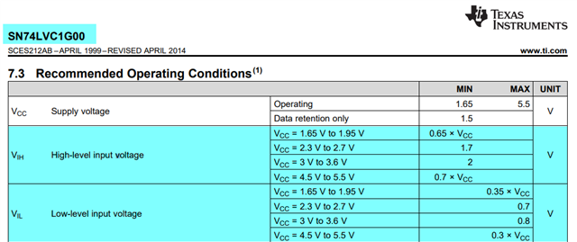
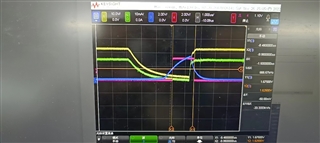
During the test, I found that the SC70 package of TI, including AND gate, NAND gate, XOR gate, positive logic gate, NOT gate, the action level of the rising and falling edge input, did not match the DATESHEET. The rising and falling input of the AND gate, NAND gate, XOR gate are around 1.5 - 1.7; the rising input of the NOT gate is around 1.9 and its falling input is around 1.0; the rising of the positive logic gate is around 2.1 and its falling is around 0.55. Could you help me figure out what may be the cause of this phenomenon?
Other relevant models:TI\SN74LVC1G14 TI\SN74LVC1G08 TI\SN74AHC1G86(CH3:Pink,CH4:Blue)
circuit: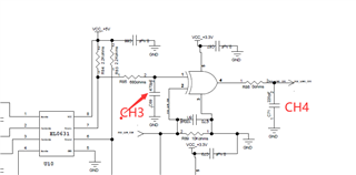
wave: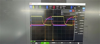 positive logic
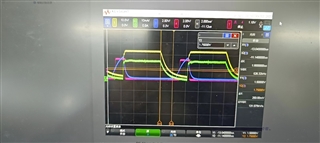 XOR
XOR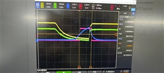 NAND
NAND
 AND
AND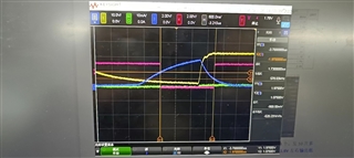 NOT
NOT