Other Parts Discussed in Thread: TLV6742, OPA2375
请注意,本文内容源自机器翻译,可能存在语法或其它翻译错误,仅供参考。如需获取准确内容,请参阅链接中的英语原文或自行翻译。
部件号:OPA2375 主题中讨论的其他部件:TLV6742,
您好,我收到了一位客户的以下问题:
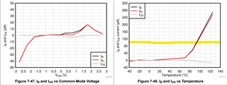
“我希望TI确认并检查OPA2375和TLV6742数据表上的差分输入阻抗。 差分模式的输入阻抗为10MOhms,共模为10GOhm。 差动输入阻抗的10MOhm对于运算放大器似乎较低。 根据数据表,这是否可以确认为正确?
此外,在最大1mV最大偏移电压/ 10Mohm差分输入阻抗的情况下,泄漏电流为0.1nA。 此泄漏电流是否正确?"
谢谢!