This thread has been locked.

If you have a related question, please click the "Ask a related question" button in the top right corner. The newly created question will be automatically linked to this question.

[参考译文] MSPM0G1518:ADC 处的 VR+>VCC

Guru**** 2522770 points
Other Parts Discussed in Thread: MSPM0G1518

请注意,本文内容源自机器翻译,可能存在语法或其它翻译错误,仅供参考。如需获取准确内容,请参阅链接中的英语原文或自行翻译。

https://e2e.ti.com/support/microcontrollers/arm-based-microcontrollers-group/arm-based-microcontrollers/f/arm-based-microcontrollers-forum/1562775/mspm0g1518-vr-vcc-at-adc

器件型号:MSPM0G1518


工具/软件:

尊敬的 TI:

我们希望使用 MSPM0G1518 进行 ADC 测量和 DAC 输出。

MCU 由 VDD 供电。

ADC/DAC 由外部基准电压 VREF 供电。

由于 DC/DC 转换器容差、VREF > VDD 可能、例如 VDD = 3.2V、VREF = 3.3V。

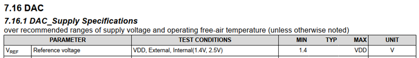
根据数据表、模拟输入电压不应超过 VDD。 此外、DAC 电源的基准电压不应超过 VDD。

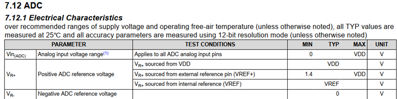
如果 ADC 正基准电压 (VR+) 大于 VDD、会发生什么情况?

此致

  • 请注意,本文内容源自机器翻译,可能存在语法或其它翻译错误,仅供参考。如需获取准确内容,请参阅链接中的英语原文或自行翻译。

    您好、

    这可能会导致电流从基准电压流向 VDD、从而损坏 MCU。 我们不建议这样做。  

    此致、

    现金好