请注意,本文内容源自机器翻译,可能存在语法或其它翻译错误,仅供参考。如需获取准确内容,请参阅链接中的英语原文或自行翻译。
部件号:AM2434 “线程:sysconfig”中讨论的其它部分
您好,
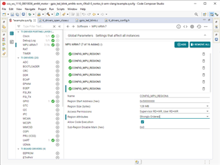
我目前正在使用 AM2343及其 SDK。 在我的项目中,我们希望通过 GPMC 外设(最终可能由 DMA 驱动)连接 DAC 和 ADC。 我们猜这是可能的,因为 DAC 和 ADC 都有一个非常接近 SRAM 的并行接口。 SDK 中还没有用于 GPMC 的驱动程序,我已经看到驱动程序计划在今年6月完成。 我等不及这一点:我的喷射器有一个非常接近的截止日期。 所以,我想自己写驱动程序。 到目前为止,我已经能够设置 GPMC 寄存器,但当我尝试向 GPMC 写入内容时,代码会出现在 Hwip_data_abort_handler 处理程序中。 我不太确定如何从 GPMC 中撰写或阅读内容... 表2-1中有与 GPMC0_DATA 区域相关的0x05000000地址。 我猜这是与 GPMC 相关的地区? 要激活这些地址,我还需要做什么? 为我的目的使用 GPMC 是否是个好主意? 最后,我只想以大约125MSPS 的速度向并行总线读取和写入16位数据...
这是我的代码:
typedef struct
{
    uint32_t REVISION;          // 0x0000
    uint32_t RESERVED_0[3];     // 0x0004
    uint32_t SYSCONFIG;         // 0x0010
    uint32_t SYSSTATUS;         // 0x0014
    uint32_t IRQSTATUS;         // 0x0018
    uint32_t IRQENABLE;         // 0x001C
    uint32_t RESERVED_1[8];     // 0x0020
    uint32_t TIMEOUT_CONTROL;   // 0x0040
    uint32_t ERR_ADDR;          // 0x0044
    uint32_t ERR_TYPE;          // 0x0048
    uint32_t RESERVED_6;        // 0x004C
    uint32_t CONFIG;            // 0x0050
    uint32_t STATUS;            // 0x0054
    uint64_t RESERVED_7;        // 0x0058
    struct
    {
        uint32_t CONFIG1;         // 0x0060
        uint32_t CONFIG2;         // 0x0064
        uint32_t CONFIG3;         // 0x0068
        uint32_t CONFIG4;         // 0x006C
        uint32_t CONFIG5;         // 0x0070
        uint32_t CONFIG6;         // 0x0074
        uint32_t CONFIG7;         // 0x0078
        uint32_t NAND_COMMAND;    // 0x007C
        uint32_t NAND_ADDRESS;    // 0x0080
        uint32_t NAND_DATA;       // 0x0084
        uint64_t RESERVED_0;      // 0x0088
    } UNIT[4];                    // 0x0090
    uint32_t RESERVED_2[48];    // 0x0120
    uint32_t PREFETCH_CONFIG1;  // 0x01E0
    uint32_t PREFETCH_CONFIG2;  // 0x01E4
    uint32_t PREFETCH_CONTROL;  // 0x01E8
    uint32_t PREFETCH_STATUS;   // 0x01EC
} GPMC_Type;

#define GPMC0_BASE (0x3B000000)
#define GPMC0 ((GPMC_Type *) GPMC0_BASE)


static Pinmux_PerCfg_t gpmcPinConfig[] = {
        {PIN_GPMC0_CLK, ( PIN_MODE(0) )},
        {PIN_GPMC0_AD0, ( PIN_MODE(0) | PIN_INPUT_ENABLE )},
        {PIN_GPMC0_AD1, ( PIN_MODE(0) | PIN_INPUT_ENABLE )},
        {PIN_GPMC0_AD2, ( PIN_MODE(0) | PIN_INPUT_ENABLE )},
        {PIN_GPMC0_AD3, ( PIN_MODE(0) | PIN_INPUT_ENABLE )},
        {PIN_GPMC0_AD4, ( PIN_MODE(0) | PIN_INPUT_ENABLE )},
        {PIN_GPMC0_AD5, ( PIN_MODE(0) | PIN_INPUT_ENABLE )},
        {PIN_GPMC0_AD6, ( PIN_MODE(0) | PIN_INPUT_ENABLE )},
        {PIN_GPMC0_AD7, ( PIN_MODE(0) | PIN_INPUT_ENABLE )},
        {PIN_GPMC0_AD8, ( PIN_MODE(0) | PIN_INPUT_ENABLE )},
        {PIN_GPMC0_AD9, ( PIN_MODE(0) | PIN_INPUT_ENABLE )},
        {PIN_GPMC0_AD10, ( PIN_MODE(0) | PIN_INPUT_ENABLE )},
        {PIN_GPMC0_AD11, ( PIN_MODE(0) | PIN_INPUT_ENABLE )},
        {PIN_GPMC0_AD12, ( PIN_MODE(0) | PIN_INPUT_ENABLE )},
        {PIN_GPMC0_AD13, ( PIN_MODE(0) | PIN_INPUT_ENABLE )},
        {PIN_GPMC0_AD14, ( PIN_MODE(0) | PIN_INPUT_ENABLE )},
        {PIN_GPMC0_AD15, ( PIN_MODE(0) | PIN_INPUT_ENABLE )},
        {PIN_GPMC0_WAIT0, ( PIN_MODE(0) | PIN_INPUT_ENABLE )},
        {PIN_GPMC0_CSN0, ( PIN_MODE(0) )},
        {PIN_GPMC0_CSN1, ( PIN_MODE(0) )},
        { PINMUX_END, PINMUX_END }, };

void GPMC_Init()
{
    // Init the clock
    SOC_moduleClockEnable(TISCI_DEV_GPMC0, 1);

    // Init the GPMC Pin
    Pinmux_config(gpmcPinConfig, PINMUX_DOMAIN_ID_MAIN);

    // Reset the GPMC
    // ??

    // Init the GPMC 0 for the DAC
    GPMC0->UNIT[0].CONFIG1 = (1 << 28)  // Enable the write multiple access
            | (1 << 27)     // Select the write synchronous
            | (1 << 24)     // Set the device burst page of 16 words
            | (1 << 12);    // Set the device size at 16 bits

    // Try a write command
    while(1)
    {
        unsigned short *addr = (unsigned short*) 0x50000000;
        (*addr) = 0x0003;


    }
}
谢谢你,
Leo