This thread has been locked.

If you have a related question, please click the "Ask a related question" button in the top right corner. The newly created question will be automatically linked to this question.

[参考译文] TMS570LC4357:F021的优化问题

Guru**** 2466550 points
Other Parts Discussed in Thread: RM48L952

请注意,本文内容源自机器翻译,可能存在语法或其它翻译错误,仅供参考。如需获取准确内容,请参阅链接中的英语原文或自行翻译。

https://e2e.ti.com/support/microcontrollers/arm-based-microcontrollers-group/arm-based-microcontrollers/f/arm-based-microcontrollers-forum/1063101/tms570lc4357-optimization-issue-for-f021

器件型号:TMS570LC4357
主题中讨论的其他器件:RM48L952

您好!

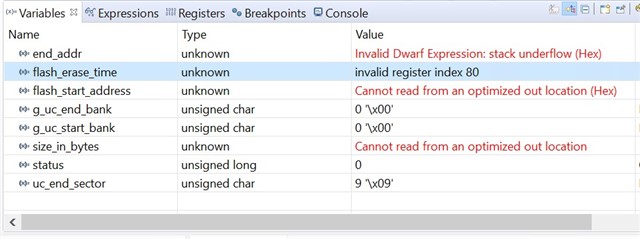
我正在尝试使用提供的库将数据擦除并编程到 L2FMC 组0和组1扇区中。 对于优化级别 O0、在使用优化级别 O1和 O2时看到两个操作都成功、看到有一个例外。 这些操作在启用指令和数据缓存之前执行。 请向我提供有关如何在对内部闪存执行操作时避免依赖优化级别的解决方案。 使用的 VCLK 为180MHz。

谢谢、

Tirumala。

  • 请注意,本文内容源自机器翻译,可能存在语法或其它翻译错误,仅供参考。如需获取准确内容,请参阅链接中的英语原文或自行翻译。

    您好、 Tirumala、

    当 opt_level=1或2时、您得到了什么错误?

  • 请注意,本文内容源自机器翻译,可能存在语法或其它翻译错误,仅供参考。如需获取准确内容,请参阅链接中的英语原文或自行翻译。
    [引用 userid="408981" URL"~/support/microcontrollers/arm-based-microcontrollers-group/arm-based-microcontrollers/f/arm-based-microcontrollers-forum/1063101/tms570lc4357-optimization-issue-for-f021优化级别为 O0时,看到使用优化级别 O1和 O2时两个操作都成功,看到存在异常。

    调用 RAM 中 F021 API 的函数以及 F021 API 函数是否都放置在 RAM 中?

    在 CCS/RM46L852中:在使用 Fapi_issueProgramming Command 时跳转至 prefetchEntry 发现:

    1.  调用 F021 API 函数的函数也需要从 RAM 运行、以避免预取中止。
    2. 当调用 F021 API 的函数位于闪存中时、尝试单步执行 F021 API 调用时会发生预取中止、但单步执行 F021 API 的指令时不会导致中止。 这表明预取中止的原因是时序敏感的、这可能解释了优化为何会起作用。
  • 请注意,本文内容源自机器翻译,可能存在语法或其它翻译错误,仅供参考。如需获取准确内容,请参阅链接中的英语原文或自行翻译。

    感谢 Gillon 的回应。

    [引用 userid="91588" URL"~/support/microcontrollers/arm-based-microcontrollers-group/arm-based-microcontrollers/f/arm-based-microcontrollers-forum/1063101/tms570lc4357-optimization-issue-for-f021/3933570 #393357"]是 RAM 中调用 F021 API 的函数、以及放置在 RAM 中的 F021 API 函数?

    之前、我已经尝试过从闪存运行的函数(调用 F021 API 函数)和从 RAM 运行的 F021 API 函数。

    根据您的回复、我尝试 使用优化级别 O1从 RAM 运行该函数(调用 F021 API 函数)。

    由于我无法在此处放置完整的代码、我想在一个实例中提供该情形。 请考虑。

    假设 函数 A ()具有 F021 API 函数调用,B ()调用 A ()。 序列是 B()->A ()--> F021 API 函数。 根据答复

    [引用 userid="91588" URL"~/support/microcontrollers/arm-based-microcontrollers-group/arm-based-microcontrollers/f/arm-based-microcontrollers-forum/1063101/tms570lc4357-optimization-issue-for-f021/3933570 #393357"]

    在 CCS/RM46L852中:在使用 Fapi_issueProgramming Command 时跳转至 prefetchEntry 发现:

    1.  调用 F021 API 函数的函数也需要从 RAM 运行、以避免预取中止。
    2. 当调用 F021 API 的函数位于闪存中时、尝试单步执行 F021 API 调用时会发生预取中止、但单步执行 F021 API 的指令时不会导致中止。 这表明预取中止的原因是时序敏感的、这可能解释了优化为何会起作用。
    [/报价]

    我已经尝试从闪存运行 B(),从 RAM 运行 A ()。 当控制必须从 B()变为 A ()时,即控制必须从闪存转换为 RAM 时,当尝试源代码步进或步进或自由运行时,代码进入异常。 仅 发生反汇编步骤、但即使如此、变量显示的错误与下面屏幕截图中的变量类似、即"无法从优化的输出位置读取"。

    这是否再次是一种计时问题?

    请考虑我为同样的问题提供的额外尝试:

    作为 F021擦除或编程的一部分、while 环路 需要等待 fmstat 寄存器变为零。 此类循环的超时根据数据表根据组号提供。 我正在使用 RTI 模块来捕获这些超时、超时的容差比数据表中提供的超时高出10%。 因此、尝试使用 F021源代码中与超时相关的函数的方法时、可以看到异常、当完全避免与超时相关的函数但我的应用中需要超时时时时时时时时、就不会出现问题、因为这是一个安全关键型系统。  您能否建议一个解决方案、在优化级别大于0且包括超时的情况下、如何避免出现这种异常?

    谢谢、

    Tirumala。

  • 请注意,本文内容源自机器翻译,可能存在语法或其它翻译错误,仅供参考。如需获取准确内容,请参阅链接中的英语原文或自行翻译。
    [引用 userid="408981" URL"~/support/microcontrollers/arm-based-microcontrollers-group/arm-based-microcontrollers/f/arm-based-microcontrollers-forum/1063101/tms570lc4357-optimization-issue-for-f021/3934195 #3934195"]I 已经尝试从闪存运行 B(),从 RAM 运行 A()。 当控制必须从 B()变为 A ()时,即控制必须从闪存转换为 RAM 时,当尝试源代码步进或步进或自由运行时,代码进入异常。 [/报价]

    如何将代码从闪存复制到 RAM?

    这似乎是以下两种情况中的一个问题:

    1. 代码如何从闪存复制到 RAM、从而导致在 RAM 中执行错误的指令。
    2. 如果 RAM 的 MMU 设置中已给出执行权限。

    请参阅 TMS570LC4357:将函数移至 RAM 以了解可能导致问题的因素。

  • 请注意,本文内容源自机器翻译,可能存在语法或其它翻译错误,仅供参考。如需获取准确内容,请参阅链接中的英语原文或自行翻译。
    [引用 userid="91588" URL"~/support/microcontrollers/arm-based-microcontrollers-group/arm-based-microcontrollers/f/arm-based-microcontrollers-forum/1063101/tms570lc4357-optimization-issue-for-f021/3935164 #3935164"]代码如何从闪存复制到 RAM?

    所有闪存功能都是使用链接器文件从 RAM 复制和运行的。

    ram_code:AT (next _load_ADDR)

    _RAM_CODE_START =.;
    *(.ram_code)
    保留(* f021_api.o (.text .text.*))
    保留(* FSM_ENABLE_MAIN_EEPROM_Sects.o (.text .text。*))
    保留(* f021_ERASE.o (.text .text.*))
    保留(* f021_init_flash_banks.o (.text .text。*))
    保留(* f021_program.o (.text .text.*))
    保留(* f021_read.o (.text .text.*))
    保留(* f021_set_active_bank.o (.text .text。*))
    保留(* f021_utils.o (.text .text.*))
    }> RAM_CODE

    RAM_CODE origin 为0x08034D00、长度为0x00005BFF、2KB 足以容纳函数。
    此外、调用闪存函数的代码使用 __attribute__((noinlinesection (".ram_code"))从 RAM 运行。

    请注意、使用的是 GCC 编译器。

    [引用 userid="91588" URL"~/support/microcontrollers/arm-based-microcontrollers-group/arm-based-microcontrollers/f/arm-based-microcontrollers-forum/1063101/tms570lc4357-optimization-issue-for-f021/3935164 #3935164"]如果 RAM 的 MMU 设置中已授予执行权限。

    MMU 中提供了执行权限。

    我还尝试了清理缓存、如中所述   

    [引用 userid="91588" URL"~/support/microcontrollers/arm-based-microcontrollers-group/arm-based-microcontrollers/f/arm-based-microcontrollers-forum/1063101/tms570lc4357-optimization-issue-for-f021/3935164 #3935164"]TMS570LC4357:将函数移动到 RAM 

    但未发现任何改进。

    请建议。

    谢谢、

    Tirumala。

  • 请注意,本文内容源自机器翻译,可能存在语法或其它翻译错误,仅供参考。如需获取准确内容,请参阅链接中的英语原文或自行翻译。
    [引用 userid="408981" URL"~/support/microcontrollers/arm-based-microcontrollers-group/arm-based-microcontrollers/f/arm-based-microcontrollers-forum/1063101/tms570lc4357-optimization-issue-for-f021/3943862 #3943862"]所有闪存功能均使用链接器文件从 RAM 复制并运行。
    Unknown 说:
    请注意使用 GCC 编译器。

    您能否确认正在使用哪个版本的 GCC 编译器?

    我不知道 GCC 运行时启动代码包含在初始化时将此类段从闪存复制到 RAM 的功能。

    您能否使用调试器检查代码是否已实际复制到 RAM?

  • 请注意,本文内容源自机器翻译,可能存在语法或其它翻译错误,仅供参考。如需获取准确内容,请参阅链接中的英语原文或自行翻译。
    [引用 userid="91588" URL"~/support/microcontrollers/arm-based-microcontrollers-group/arm-based-microcontrollers/f/arm-based-microcontrollers-forum/1063101/tms570lc4357-optimization-issue-for-f021/3943895 #3943895"]我不知道 GCC 运行时启动代码包含在初始化时将此类段从闪存复制到 RAM 的功能。

    回顾  RM48L952的示例项目 RM48L952_GCC_FEE 读写、该项目将 F021 API 代码从闪存复制到 SRAM、 sys_main.c 必须将 F021代码从闪存复制到 SRAM、如下所示:

    /* Symbols defined by linker script to copy flash API functions from the load address in flash to the run address in sram */
    extern char _sflashAPI;
    extern char _siflashAPI;
    extern char _eflashAPI;
    
    /* USER CODE END */
    
    /** @fn void main(void)
    *   @brief Application main function
    *   @note This function is empty by default.
    *
    *   This function is called after startup.
    *   The user can use this function to implement the application.
    */
    
    /* USER CODE BEGIN (2) */
    /* USER CODE END */
    
    void main(void)
    {
    /* USER CODE BEGIN (3) */
        unsigned int BlockNumber;
        unsigned int BlockOffset, Length;
        unsigned char *Read_Ptr=read_data;
    
        unsigned int loop;
    
        /* Copy flash API functions from flash to RAM */
        memcpy (&_sflashAPI, &_siflashAPI, &_eflashAPI - &_sflashAPI);

    sys_link.ld  链接器脚本的各节中包含以下内容:

      .flashAPI :
      {
        . = ALIGN(4);
    
        _sflashAPI = .;         /* create a global symbol at data start */
        *Fapi_UserDefinedFunctions.o (.text*)
        *F021_API_CortexR4_LE_V3D16.lib:* (.text*)
    
        . = ALIGN(4);
        _eflashAPI = .;            /* define a global symbol at data end */
      } >RAM AT> FLASH_API

    以上示例可能有所帮助。

        /* used by the startup to initialize flashAPI */
       _siflashAPI = LOADADDR(.flashAPI);
    
      .flashAPI :
      {
        . = ALIGN(4);
    
        _sflashAPI = .;         /* create a global symbol at data start */
        *Fapi_UserDefinedFunctions.o (.text*)
        *F021_API_CortexR4_LE_V3D16.lib:* (.text*)
    
        . = ALIGN(4);
        _eflashAPI = .;            /* define a global symbol at data end */
      } >RAM AT> FLASH_API

  • 请注意,本文内容源自机器翻译,可能存在语法或其它翻译错误,仅供参考。如需获取准确内容,请参阅链接中的英语原文或自行翻译。

    感谢您的回应、Chester Gillon。

     前面提到的链接器脚本与我在之前的响应中提到的脚本类似、其中与 F021功能相关的所有目标文件都被复制到 RAM 中。 在调试时、我可以看到这些函数从 RAM 位置运行。

  • 请注意,本文内容源自机器翻译,可能存在语法或其它翻译错误,仅供参考。如需获取准确内容,请参阅链接中的英语原文或自行翻译。

    切斯特·吉隆、您能 不能告诉我 F021操作优化问题的可能解决方案。

    提前感谢您!

  • 请注意,本文内容源自机器翻译,可能存在语法或其它翻译错误,仅供参考。如需获取准确内容,请参阅链接中的英语原文或自行翻译。

    切斯特·吉隆、您好 吗?请告诉我 F021操作优化问题的可能解决方案(如果有)。

    提前感谢您!

  • 请注意,本文内容源自机器翻译,可能存在语法或其它翻译错误,仅供参考。如需获取准确内容,请参阅链接中的英语原文或自行翻译。
    [引用 userid="408981" URL"~/support/microcontrollers/arm-based-microcontrollers-group/arm-based-microcontrollers/f/arm-based-microcontrollers-forum/1063101/tms570lc4357-optimization-issue-for-f021/3959171 #3959171"]您好 Chester Gillon ,您能不能告诉我 F021操作优化问题的可能解决方案(如果有)。

    我无法从可用信息中确定优化问题的原因。 您是否能够发布显示故障的示例程序?

  • 请注意,本文内容源自机器翻译,可能存在语法或其它翻译错误,仅供参考。如需获取准确内容,请参阅链接中的英语原文或自行翻译。

    切斯特·吉隆、您好!

    由于我无法在这里提供完整的代码、我将提供示例代码以及解释所执行功能的注释。 仅提供闪存擦除和编程调用。 请考虑。

        #define CONST_3FF   __asm__ __volatile__("CONST_3FF  .word 0x3ff");
        #define CONST_7FFF  __asm__ __volatile__("CONST_7FFF .word 0x00007fff");
    
        #define CACHE_CLEAN __asm__ __volatile__(" MRC p15, #1, r0, c0, c0, #1 \n"  \
        " ANDS R3, R0, #0x07000000 \n"     \
        " MOV R3, R3, LSR #23 \n"          \
        " BEQ Finished \n"                 \
        " MOV R10, #0 \n"                  \
        "Loop1: \n"                        \
        " ADD R2, R10, R10, LSR #1 \n"     \
        " MOV R1, R0, LSR R2 \n"           \
        " AND R1, R1, #7 \n"               \
        " CMP R1, #2 \n"                   \
        " BLT Skip \n"                     \
        " MCR p15, #2, R10, c0, c0, #0 \n" \
        " ISB \n"                          \
        " MRC p15, #1, R1, c0, c0, #0 \n"  \
        " AND R2, R1, #7 \n"               \
        " ADD R2, R2, #4 \n"               \
        " LDR R4, = 0x3FF \n"           \
        " ANDS R4, R4, R1, LSR #3 \n"      \
        " CLZ R5, R4 \n"                   \
        " MOV R9, R4 \n"                   \
        "Loop2: \n"                        \
        " LDR R7, = 0x7FFF \n"           \
        " ANDS R7, R7, R1, LSR #13 \n"     \
        "Loop3: \n"                        \
        " ORR R11, R10, R9, LSL R5 \n"     \
        " ORR R11, R11, R7, LSL R2 \n"     \
        " MCR p15, #0, R11, c7, c10, #2 \n"\
        " SUBS R7, R7, #1 \n"              \
        " BGE Loop3 \n"                    \
        " SUBS R9, R9, #1 \n"              \
        " BGE Loop2 \n"                    \
        "Skip: \n"                         \
        " ADD R10, R10, #2 \n"             \
        " CMP R3, R10 \n"                  \
        " BGT Loop1 \n"                    \
        " DSB \n"                          \
        "Finished:")
    
     
    void cache_clean()
    {
    	CACHE_CLEAN;
    	return;
    }
    
    
    void entry_point()
    {
        // - pre-initializations for data, BSS sections and constuctors
    	// - Copy code from ROM to RAM, the code that should be executed from RAM
    
        // - Enable CPU bus event export
    
        // - reset handler for the types of reset
    
        // - Work around after checking if there were ESM group3 errors during power-up and clearing it
        //   These could occur during eFuse auto-load or during reads from flash OTP
        //   during power-up. Device operation is not reliable and not recommended
        //   in this case.
    
        // - setting up the PLL
    
        // - Release the peripherals from reset and enable clocks to all peripherals.
    
        // - PINMUX initialization and settings
    
        // - Initializing and Setting up the flash with HCLK 
    
        // - Trimming of LPO
    	
        // - Clock mapping
    
        // - Power on initialization of system clock
    
        // - Configure and setup the EMIF
    
        cache_clean();
    
        // - Pre- Initializations for data, BSS sections and constuctors
    
        // - Copy code from ROM to RAM, the code that should be executed from RAM
    
    
        flash_op();
    }
    
    
    uint32 flash_data[256 * 8];
    
    __attribute__((noinline, section(".ram_code"))) void flash_op(void)  // To run from the RAM location. Please find the attached code of linker file after the F021 API functions 
    {
        // - Initializing and Setting up the flash with HCLK 
    
        // - initialization of system clock
    
        // - Perform L2 SRAM single bit and multi bit ECC tests
    
        // - Perform flash single bit and multi bit ECC tests
    
        // - Install exception handlers in RAM location
    
        // - Initialize VIM
    
        // - Initialize ESM to configure system response to error conditions signaled to the ESM group1
    
        // - MPU initialization as below:
        //       Internal flash - Region 0 -  size 4MB - Outer and Inner write-through, no write-allocate non-shareable type and Privileged/User read-only mode.
        //       Internal SRAM  - Region 1 -  size 512KB - Outer and Inner write-through, no write-allocate non-shareable type and with full access mode.
        //       Internal Flash (Flash ECC, OTP and EEPROM accesses) - Region 2 - size 8MB - device, non-shareable type, writes in User mode generate permission faults access and never executes.
    	
    	// Note: The remaining MPU initializations are excluded here
    
        for(uint32 i = 0UL; i < (256UL * 8UL); i++)
        {
            flash_data[i]   = 0xAA552233UL;
            flash_data[i+1] = 0x33449988UL;
            flash_data[i+2] = 0xAA125623UL;
            flash_data[i+3] = 0x34459189UL;
            i += 3;
        }
    
        if(FapiBlockErase(0x60000, 8192UL) /* Erase the flash from 0x60000 of size 8MB.*/)
        {
            FapiBlockProgramEcc(0x60000, &flash_data, (4UL * 1024UL * 2UL));
        }
    
        // - Enable Instruction cache and data cache
        
        while(1);
    }

    和闪存 API 函数如下所示:

    uint32 FapiBlockErase(uint32 FlashStartAddress, uint32 SizeInBytes)
    {
        // Compute the bank number based on the start address and the size provided. 
    
        // Initialize the F021 based on the start bank where the flash start address lies and the end bank where the end address (calculated based on the size) resides.
    	
    	// For each sector, perform erase operation. After performing erase operation of each sector, status of the FMSTAT register is collected if it becomes zero within the provided timeouts. If the time is exceeding the provided limit, then the further erase of sectors is not performed and the status of erase operation is not successful.
    	// Based on the computed bank number, the timeouts are provided as below:
        // Maximum erase time for main banks is 4.4 sec for sector erase as per the datasheet.
        // Maximum erase time for EEPROM is 8.8 sec for sector erase as per the datasheet.
         
    	// Return the status of the erase operation.
    }
    
    uint32 FapiBlockProgramEcc(uint32 FlashStartAddress, uint32 DataStartSddress, uint32 SizeInBytes)
    {
        // 1. Compute the bank number based on the start address and the size provided.  
    
        // 2. If the flash bank has been initialized in flash erase function, do not perform the initialization. Otherwise, initialize the flash based on the start bank where the flash start address lies and the end bank where the end address (calculated based on the size) resides.
    
        // 3. If the initialization is done, perform the programming byte by byte using the FlashStartAddress, DataStartSddress and SizeInBytes. After performing program operation on each byte, status of the FMSTAT register is collected if it becomes zero within the provided timeouts. If the time is exceeding the provided limit, then the further programming of sectors is not performed and the status of programming operation is not successful.
    	
    	// 3. Based on the computed bank number, the timeouts are provided as below:
        //    Maximum program time for 4MB internal flash main banks is 21.23 sec as per the datasheet.
        //    Maximum program time for 128KB EEPROM bank is 2.86 sec as per the datasheet.
    
    	//    Return the status of the program operation.
    }
    

    上述闪存 API 函数和所有与闪存相关的文件/操作都被复制到 RAM 中并从 RAM 中执行。 用于从 RAM 执行的链接器脚本如下所示:
    ram_code:AT (next _load_ADDR)

    _RAM_CODE_START =.;
    *(.ram_code)
    保留(* F021Api.o (.text .text.*))
    保留(* FSM_ENABLE_MAIN_EEPROM_Sects.o (.text .text。*))
    保留(* f021_ERASE.o (.text .text.*))
    保留(* f021_init_flash_banks.o (.text .text。*))
    保留(* f021_program.o (.text .text.*))
    保留(* f021_read.o (.text .text.*))
    保留(* f021_set_active_bank.o (.text .text。*))
    保留(* f021_utils.o (.text .text.*))
    }> RAM_CODE
    _RAM_CODE_SIZE =(SIZEOF (.ram_code)/ 4);

    该代码使用 GCC 编译器4.2.3版进行编译。 用户可以选择优化级别。 当使用0级时、擦除/编程由提供的超时完成。 没有问题。

    当优化级别提高(我尝试使用级别1和2)时、我会看到这些操作中的问题。 因此、我尝试删除了超时的用法、我可以在其中完成这些操作(使用级别1和级别2)。 由于系统对安全至关重要、因此需要实施超时。 超时在 RTI 定时器模块的帮助下使用。

    此外,基于您之前的响应,包括 cache_clear(),这对解决问题没有任何影响。

    如果 需要任何其他信息、请告知我。

    谢谢、
    Tirumala。

  • 请注意,本文内容源自机器翻译,可能存在语法或其它翻译错误,仅供参考。如需获取准确内容,请参阅链接中的英语原文或自行翻译。
    [引用 userid="408981" URL"~/support/microcontrollers/arm-based-microcontrollers-group/arm-based-microcontrollers/f/arm-based-microcontrollers-forum/1063101/tms570lc4357-optimization-issue-for-f021/3960888 #3960888">因此我尝试删除了超时的用法,以便能够完成这些操作(级别1和级别2)。 由于系统对安全至关重要、因此需要实施超时。 超时在 RTI 定时器模块的帮助下使用。[/quot]

    您能否显示执行超时操作的代码?

    这可能类似于中断处理程序与代码其余部分共享的变量缺少 volatile 限定符。

  • 请注意,本文内容源自机器翻译,可能存在语法或其它翻译错误,仅供参考。如需获取准确内容,请参阅链接中的英语原文或自行翻译。

    当然。  

    这是代码。

       union FMSTAT
       {
          uint32 u32Register; // Module Status Register, bits 31:0 
          struct
          {
             uint32 _FMSTAT_Reserved_31_18  :14;// !< Reserved, bits 31:18 
             uint32 RVSUSP                  :1; // !< Read Verify Suspend, bit 17 
             uint32 RDVER                   :1; // !< Read Verify command currently underway, bit 16 
             uint32 RVF                     :1; // !< Read Verify Failure, bit 15 
             uint32 ILA                     :1; // !< Illegal Address, bit 14 
             uint32 DBT                     :1; // !< Disturbance Test Fail, bit 13 
             uint32 PGV                     :1; // !< Program verify, bit 12 
             uint32 PCV                     :1; // !< Precondidition verify, bit 11 
             uint32 EV                      :1; // !< Erase verify, bit 10 
             uint32 CV                      :1; // !< Compact Verify, bit 9 
             uint32 BUSY                    :1; // !< Busy, bit 8 
             uint32 ERS                     :1; // !< Erase Active, bit 7 
             uint32 PGM                     :1; // !< Program Active, bit 6 
             uint32 INVDAT                  :1; // !< Invalid Data, bit 5 
             uint32 CSTAT                   :1; // !< Command Status, bit 4 
             uint32 VOLSTAT                 :1; // !< Core Voltage Status, bit 3 
             uint32 ESUSP                   :1; // !< Erase Suspend, bit 2 
             uint32 PSUSP                   :1; // !< Program Suspend, bit 1 
             uint32 SLOCK                   :1; // !< Sector Lock Status, bit 0 
          } FMSTAT_BITS;
       } FmStat;
    
    #define F021_CPU0_REGISTER_ADDRESS 0xFFF87000U
    
    typedef Fapi_FmcRegistersType* pFapi_FmcRegistersType;
    #define FLASH_CONTROL_REGISTER (reinterpret_cast<pFapi_FmcRegistersType>(F021_CPU0_REGISTER_ADDRESS))
    
    #define FAPI_GET_FSM_STATUS (FLASH_CONTROL_REGISTER->FmStat.u32Register)
    #define FAPI_STATUS_SUCCESS 0
    
    // get_time()- Collects the current time
    
    // time(since) - Gets the difference between the time period at the instant and the time passed as argument
    
    static uint32 wait_for_fsm(uint32 flash_operation_time)
    {
        uint32 status = 1U;
    
        uint64 start_time = get_time();
    
        // Expected to complete the while loop with in the flash operation time.
        while((static_cast<uint32>(time_since(start_time)) < flash_operation_time) && (status == 0))
    	{
    		status = ((static_cast<FapiStatusType>(FAPI_GET_FSM_STATUS)) == (static_cast<FapiStatusType>(FAPI_STATUS_SUCCESS)));
    	}
    
        return status;
    }
    
    
    // Initialize the flash bank and activate the sectors
    extern uint32 fapi_block_erase(uint32 flash_start_address, uint32 size_in_bytes)
    {
        uint8  i = 0U;
        uint8 g_uc_start_bank = 0U;
        uint8 g_uc_end_bank = 0U;
        uint8 uc_start_sector = 0U;
        uint8 uc_end_sector = 0U;
        uint32 end_addr = 0U;
        uint32 status = 0U;
    
        // Maximum erase time for internal flash is 4sec for sector erase as per the datasheet.
        uint32 flash_erase_time = 4000U + 400U; // time out with 10% tolerance
    
        end_addr = flash_start_address + size_in_bytes;
        uc_start_sector = compute_bank_number(flash_start_address, &g_uc_start_bank); // Computes the bank number where the flash start address lies
    
        // flash_sector array is a hardcoded value having th sectors corresponding to the banks and size.
        for (i = uc_start_sector; (i < NUMBEROFSECTORS); i++)
        {
            if (end_addr <= (reinterpret_cast<uint32> (flash_sector[i].start) + flash_sector[i].length) )
            {
                g_uc_end_bank = flash_sector[i].bank_number;
                uc_end_sector = i;
                break;
            }
        }
    
        // Maximum erase time for eeprom is 8sec for sector erase as per the datasheet.
        if(g_uc_start_bank == 7U)
        {
            flash_erase_time = 8000U + 800U; // time out with 10% tolerance
        }
    
        status = fapi_init(g_uc_start_bank, g_uc_end_bank);
    
        for (i = uc_start_sector; ( (i < (uc_end_sector + 1U)) && (1U == status) ); i++)
        {
            fapi_issue_async_cmd_with_address(FAPI_ERASE_SECTOR, reinterpret_cast<uint32 *>(flash_sector[i].start));
            //Flash erase timeout includes both state machine overhead and flash erase time
            status = wait_for_fsm(flash_erase_time);    // This Function waits until the FMSTAT register becomes zero until the flash erase time
        }
    
        return (status);
    }
    
    
    extern uint32 fapi_block_program_ecc(uint32 flash_start_address, uint32 data_start_address, uint32 size_in_bytes)
    {
    	register uint32 src = data_start_address;
        register uint32 dst = flash_start_address;
        uint8 bytes = 8U;
        uint32 status = 1U;
        uint8 g_uc_start_bank = 0U;
    
        // Maximum program time for 4MB internal flash is 21.3 sec as per the datasheet.
        uint32 flash_program_time = 21300U + 2130U; // time out with 10% tolerance
    
        uint8 uc_start_sector = compute_bank_number(flash_start_address, &g_uc_start_bank);
        
        if (size_in_bytes < 8U)
            bytes = static_cast<uint8>(size_in_bytes);
    
        //  The flash bank has been initialized in flash erase function.
        if (g_ul_bank_initialized != 1U)
        {
            uint8  i = 0U;
            uint8 g_uc_end_bank = 0U;
            uint32 end_addr = flash_start_address + size_in_bytes;
    
            uint8 loop_break_variable = 0U;
            for (i = uc_start_sector; (i < NUMBEROFSECTORS) && (!loop_break_variable); i++)
            {
                if (end_addr <= (reinterpret_cast<uint32> (flash_sector[i].start) + flash_sector[i].length) )
                {
                    g_uc_end_bank = flash_sector[i].bank_number;
                    loop_break_variable += 1U;
                }
            }
            status = fapi_init(g_uc_start_bank, g_uc_end_bank);
        }
    
        // Maximum program time for 128KB eeprom bank is 2.6 sec as per the datasheet.
        if(g_uc_start_bank == 7U)
        {
            flash_program_time = 2600U + 260U; // time out with 10% tolerance
        }
    
        while( (size_in_bytes > 0U) && (1U == status) )
        {
            fapi_issue_programming_command(reinterpret_cast< uint32 *>(dst),
                                         reinterpret_cast< uint8 *>(src),
                                         bytes);
            status = wait_for_fsm(flash_program_time); // This Function waits until the FMSTAT register becomes zero until the flash erase time
    
            if(1U == status)
            {
                src += bytes;
                dst += bytes;
                size_in_bytes -= bytes;
    
                if ( size_in_bytes < 8U)
                {
                    bytes = static_cast<uint8>(size_in_bytes);
                }
            }
        }
        return(status);
    }

    代码采用 CPP。 如前所述、 当(TIME_INAS (START_TIME))< FLASH_OPERAY_TIME)未在 WAIT_TO_FSM ()中使用时不会出现问题。

    请告诉我、除了提供的代码之外、是否需要其他信息。

  • 请注意,本文内容源自机器翻译,可能存在语法或其它翻译错误,仅供参考。如需获取准确内容,请参阅链接中的英语原文或自行翻译。

    切斯特·吉隆、您好、请告诉我这些信息是否足够。

    谢谢你。