请注意,本文内容源自机器翻译,可能存在语法或其它翻译错误,仅供参考。如需获取准确内容,请参阅链接中的英语原文或自行翻译。
器件型号:TM4C1294NCPDT 主题中讨论的其他器件:TM4C129XNCZAD
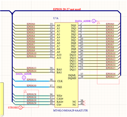
因此、连接 到 EPI 的 MT48LC4M16A2P-6A 存在问题。
我一直在向 SDRAM 写入一个字节、但读取的值并不总是与写入的值相同。 我已经创建了一个 for 循环、以便在时将一个数据写入到 EPI 地址:
for (uint_fast32_t i = 0; i < SDRAM_END_ADDRESS;++i)
{
    base[i] = (uint8_t)i;
}
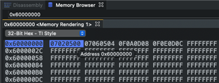
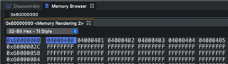
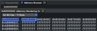
使用调试器、我可以看到、对于索引1、3、9、11、17、 19...
1变为5
3变为7
9变为13
11变为15
因此、在这些 情况下、3位始终为1。 存储器为16位、具有1Meg x 16 x 4组、行访问需要12位、列需要8位。 EPI 是否存在问题、以及该 SDRAM 中的存储器是如何组织的?
下面是配置(GPIO 外设已全部启用):
//
    // The EPI0 peripheral must be enabled for use.
    //
    SysCtlPeripheralEnable(SYSCTL_PERIPH_EPI0);


    //
    // This step configures the internal pin muxes to set the EPI pins for use
    // with EPI.  Please refer to the datasheet for more information about pin
    // muxing.  Note that EPI0S27:20 are not used for the EPI SDRAM
    // implementation.
    // TODO: Update this section based upon the EPI pin assignment on your
    // target part.
    //

    //
    // EPI0S00 ~ EPI0S03 : H0 ~ 3
    //
    ui32Val = HWREG(GPIO_PORTH_BASE + GPIO_O_PCTL);
    ui32Val &= 0xFFFF0000;
    ui32Val |= 0x0000FFFF;
    HWREG(GPIO_PORTH_BASE + GPIO_O_PCTL) = ui32Val;

    //
    // EPI0S4 ~ EPI0S7: C4 ~ 7
    //
    ui32Val = HWREG(GPIO_PORTC_BASE + GPIO_O_PCTL);
    ui32Val &= 0x0000FFFF;
    ui32Val |= 0xFFFF0000;
    HWREG(GPIO_PORTC_BASE + GPIO_O_PCTL) = ui32Val;

    //
    // EPI0S8 ~ EPI0S9: A6 ~ 7
    //
    ui32Val = HWREG(GPIO_PORTA_BASE + GPIO_O_PCTL);
    ui32Val &= 0x00FFFFFF;
    ui32Val |= 0xFF000000;
    HWREG(GPIO_PORTA_BASE + GPIO_O_PCTL) = ui32Val;

    //
    // EPI0S10 ~ EPI0S11: G0 ~ 1
    //
    ui32Val = HWREG(GPIO_PORTG_BASE + GPIO_O_PCTL);
    ui32Val &= 0xFFFFFF00;
    ui32Val |= 0x000000FF;
    HWREG(GPIO_PORTG_BASE + GPIO_O_PCTL) = ui32Val;

    //
    // EPI0S12 ~ EPI0S15: M0 ~ 3
    //
    ui32Val = HWREG(GPIO_PORTM_BASE + GPIO_O_PCTL);
    ui32Val &= 0xFFFF0000;
    ui32Val |= 0x0000FFFF;
    HWREG(GPIO_PORTM_BASE + GPIO_O_PCTL) = ui32Val;

    //
    // EPI0S16 ~ EPI0S19: L0 ~ 3
    //
    ui32Val = HWREG(GPIO_PORTL_BASE + GPIO_O_PCTL);
    ui32Val &= 0xFFFF0000;
    ui32Val |= 0x0000FFFF;
    HWREG(GPIO_PORTL_BASE + GPIO_O_PCTL) = ui32Val;

    //
    // EPI0S28 : B3
    //
    ui32Val = HWREG(GPIO_PORTB_BASE + GPIO_O_PCTL);
    ui32Val &= 0xFFFF0FFF;
    ui32Val |= 0x0000F000;
    HWREG(GPIO_PORTB_BASE + GPIO_O_PCTL) = ui32Val;

    //
    // EPI0S29 ~ EPI0S30: N2 ~ 3
    //
    ui32Val = HWREG(GPIO_PORTN_BASE + GPIO_O_PCTL);
    ui32Val &= 0xFFFF00FF;
    ui32Val |= 0x0000FF00;
    HWREG(GPIO_PORTN_BASE + GPIO_O_PCTL) = ui32Val;

    //
    // EPI0S31 : K5
    //
    ui32Val = HWREG(GPIO_PORTK_BASE + GPIO_O_PCTL);
    ui32Val &= 0xFF0FFFFF;
    ui32Val |= 0x00F00000;
    HWREG(GPIO_PORTK_BASE + GPIO_O_PCTL) = ui32Val;


    //
    // Configure the GPIO pins for EPI mode.  All the EPI pins require 8mA
    // drive strength in push-pull operation.  This step also gives control of
    // pins to the EPI module.
    //
    GPIOPinTypeEPI(GPIO_PORTA_BASE, EPI_PORTA_PINS);
    GPIOPinTypeEPI(GPIO_PORTB_BASE, EPI_PORTB_PINS);
    GPIOPinTypeEPI(GPIO_PORTC_BASE, EPI_PORTC_PINS);
    GPIOPinTypeEPI(GPIO_PORTG_BASE, EPI_PORTG_PINS);
    GPIOPinTypeEPI(GPIO_PORTH_BASE, EPI_PORTH_PINS);
    GPIOPinTypeEPI(GPIO_PORTK_BASE, EPI_PORTK_PINS);
    GPIOPinTypeEPI(GPIO_PORTL_BASE, EPI_PORTL_PINS);
    GPIOPinTypeEPI(GPIO_PORTM_BASE, EPI_PORTM_PINS);
    GPIOPinTypeEPI(GPIO_PORTN_BASE, EPI_PORTN_PINS);


    // Our current system clock faster than we can drive the SDRAM clock
    EPIDividerSet(EPI0_BASE, 1);


    //
    // Sets the usage mode of the EPI module.  For this example we will use
    // the SDRAM mode to talk to the external 16MB SDRAM module.
    //
    EPIModeSet(EPI0_BASE, EPI_MODE_SDRAM);


    //
    // Configure the SDRAM mode.  We configure the SDRAM according to our core
    // clock frequency.  We will use the normal (or full power) operating
    // state which means we will not use the low power self-refresh state.
    // Set the SDRAM size to 8MB with a refresh interval of 900 clock ticks.
    //
    EPIConfigSDRAMSet(EPI0_BASE, (EPI_SDRAM_CORE_FREQ_50_100 | EPI_SDRAM_FULL_POWER |
                      EPI_SDRAM_SIZE_64MBIT), 900);

    //
    // Set the address map.  The EPI0 is mapped from 0x60000000 to 0x01000000.
    // For this example, we will start from a base address of 0x60000000 with
    // a size of 256MB.  Although our SDRAM is only 64MB, there is no 64MB
    // aperture option so we pick the next larger size.
    //
    EPIAddressMapSet(EPI0_BASE, EPI_ADDR_RAM_SIZE_16MB | EPI_ADDR_RAM_BASE_6);

    //
    // Wait for the SDRAM wake-up to complete by polling the SDRAM
    // initialization sequence bit.  This bit is true when the SDRAM interface
    // is going through the initialization and false when the SDRAM interface
    // it is not in a wake-up period.
    //
    while(HWREG(EPI0_BASE + EPI_O_STAT) &  EPI_STAT_INITSEQ)
    {
    }
BR JHi