请注意,本文内容源自机器翻译,可能存在语法或其它翻译错误,仅供参考。如需获取准确内容,请参阅链接中的英语原文或自行翻译。
器件型号:TMS570LC4357 主题中讨论的其他器件:HALCOGEN
大家好:
我现在正在对从75MHz 到100MHz 的 EMIF 总线的速度进行编程。 通过 halcogen、我已经成功地将 EMIF 的频率更改为100MHz、并通过示波器测试频率。
然后我想使用 RTI 模块充当"时间戳"来测试从 SRAM 到 SDRAM 的数据复制。 在本例中、我还会重新配置保持5MHz 频率的 RTI 模块。 测试代码如下:
#define rtos_realTimer         (*(volatile int*)0xFFFFFC10U)
/* USER CODE END */
int Wtbuf[1024]={0};
int  timedely,after;

int main(void)
{
/* USER CODE BEGIN (3) */
    rtiInit();
    sciInit();
    sciSendByte(sciREG4,0x34);
    int *prt=NULL;
    int before,i;
    prt =(int*)0x80000000;
    memset(Wtbuf,0,sizeof(Wtbuf));

    for(i=0;i<1024;i++)
    {
      Wtbuf[i]=i+0x5A5A0000;
    }

    before = rtos_realTimer;
    for(i=0;i<1024;i++)
    {
         prt[i] =Wtbuf[i];
    }
    after =rtos_realTimer;
    timedely =(after - before);

/* USER CODE END */

    return 0;
}
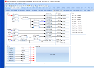
在我的映射时钟中、HCLK 为100MHz、VCLK1=VCLK2=VCL3=100Mhz。
void mapClocks(void)
{
    uint32 SYS_CSVSTAT, SYS_CSDIS;

/* USER CODE BEGIN (11) */
/* USER CODE END */

    /** @b Initialize @b Clock @b Tree: */
    /** - Setup system clock divider for HCLK */

    systemREG2->HCLKCNTL = 2U;

    /** - Disable / Enable clock domain */
    systemREG1->CDDIS = (uint32)((uint32)0U << 4U ) /* AVCLK1 , 1 - OFF, 0 - ON */
                      | (uint32)((uint32)1U << 5U ) /* AVCLK2 , 1 - OFF, 0 - ON */
                      | (uint32)((uint32)0U << 8U ) /* VCLK3 , 1 - OFF, 0 - ON */
                      | (uint32)((uint32)0U << 9U ) /* VCLK4 , 1 - OFF, 0 - ON */
                      | (uint32)((uint32)0U << 10U) /* AVCLK3 , 1 - OFF, 0 - ON */
                      | (uint32)((uint32)0U << 11U); /* AVCLK4 , 1 - OFF, 0 - ON */


    /* Always check the CSDIS register to make sure the clock source is turned on and check
     * the CSVSTAT register to make sure the clock source is valid. Then write to GHVSRC to switch the clock.
     */
    /** - Wait for until clocks are locked */
    SYS_CSVSTAT = systemREG1->CSVSTAT;
    SYS_CSDIS = systemREG1->CSDIS;
    while ((SYS_CSVSTAT & ((SYS_CSDIS ^ 0xFFU) & 0xFFU)) != ((SYS_CSDIS ^ 0xFFU) & 0xFFU))
    {
        SYS_CSVSTAT = systemREG1->CSVSTAT;
        SYS_CSDIS = systemREG1->CSDIS;
    } /* Wait */

/* USER CODE BEGIN (12) */
/* USER CODE END */

    /** - Map device clock domains to desired sources and configure top-level dividers */
    /** - All clock domains are working off the default clock sources until now */
    /** - The below assignments can be easily modified using the HALCoGen GUI */

    /** - Setup GCLK, HCLK and VCLK clock source for normal operation, power down mode and after wakeup */
    systemREG1->GHVSRC = (uint32)((uint32)SYS_PLL1 << 24U)
                       | (uint32)((uint32)SYS_PLL1 << 16U)
                       | (uint32)((uint32)SYS_PLL1 << 0U);

    /** - Setup RTICLK1 and RTICLK2 clocks */
    systemREG1->RCLKSRC = (uint32)((uint32)1U << 24U)        /* RTI2 divider (Not applicable for lock-step device)  */
                        | (uint32)((uint32)SYS_VCLK << 16U) /* RTI2 clock source (Not applicable for lock-step device) */
                        | (uint32)((uint32)2U << 8U)         /* RTI1 divider */
                        | (uint32)((uint32)SYS_VCLK << 0U); /* RTI1 clock source */

    /** - Setup asynchronous peripheral clock sources for AVCLK1 and AVCLK2 */
    systemREG1->VCLKASRC = (uint32)((uint32)SYS_VCLK << 8U)
                         | (uint32)((uint32)SYS_VCLK << 0U);

    /** - Setup synchronous peripheral clock dividers for VCLK1, VCLK2, VCLK3 */
    systemREG1->CLKCNTL  = (systemREG1->CLKCNTL & 0xF0FFFFFFU)
                         | (uint32)((uint32)0U << 24U);
    systemREG1->CLKCNTL  = (systemREG1->CLKCNTL & 0xFFF0FFFFU)
                         | (uint32)((uint32)0U << 16U);

    systemREG2->CLK2CNTRL = (systemREG2->CLK2CNTRL & 0xFFFFFFF0U)
                         | (uint32)((uint32)0U << 0U);

    systemREG2->VCLKACON1 =  (uint32)((uint32)(2U - 1U) << 24U)
                           | (uint32)((uint32)0U << 20U)
                           | (uint32)((uint32)SYS_VCLK << 16U)
                           | (uint32)((uint32)(1U - 1U) << 8U)
                           | (uint32)((uint32)0U << 4U)
                           | (uint32)((uint32)SYS_VCLK << 0U);

/* USER CODE BEGIN (13) */
/* USER CODE END */

    /* Now the PLLs are locked and the PLL outputs can be sped up */
    /* The R-divider was programmed to be 0xF. Now this divider is changed to programmed value */
    systemREG1->PLLCTL1 = (systemREG1->PLLCTL1 & 0xE0FFFFFFU) | (uint32)((uint32)(1U - 1U) << 24U);
    /*SAFETYMCUSW 134 S MR:12.2 <APPROVED> " Clear and write to the volatile register " */
    systemREG2->PLLCTL3 = (systemREG2->PLLCTL3 & 0xE0FFFFFFU) | (uint32)((uint32)(1U - 1U) << 24U);

    /* Enable/Disable Frequency modulation */
    systemREG1->PLLCTL2 |= 0x00000000U;

/* USER CODE BEGIN (14) */
/* USER CODE END */

}
void rtiInit(void)
{
    /** - Setup NTU source, debug options and disable both counter blocks */
       rtiREG1->GCTRL = 0x80000000u;

       /** - Setup timebase for free running counter 0 */
       rtiREG1->TBCTRL = 0x00000000u;

       /** - Enable/Disable capture event sources for both counter blocks */
       rtiREG1->CAPCTRL = 0x00000000u;

       /** - Setup input source compare 0-3 */
       rtiREG1->COMPCTRL = 0x00000000u;

       /** - Reset up counter 0 */
       rtiREG1->CNT[0U].UCx = 0x00000000u;

       /** - Reset free running counter 0 */
       rtiREG1->CNT[0U].FRCx = 0x00000000u;

       /** - Setup up counter 0 compare value
       *     - 0x00000000: Divide by 2^32
       *     - 0x00000001-0xFFFFFFFF: Divide by (CPUC0 + 1)
       */
       rtiREG1->CNT[0U].CPUCx = 19U; // RTICLK = 100MHz; Counter0 clk = 5MHz  200ns


       /** - Reset up counter 1 */
       rtiREG1->CNT[1U].UCx = 0x00000000u;

       /** - Reset free running counter 1 */
       rtiREG1->CNT[1U].FRCx  = 0x00000000u;

       /** - Setup up counter 1 compare value
       *     - 0x00000000: Divide by 2^32
       *     - 0x00000001-0xFFFFFFFF: Divide by (CPUC1 + 1)
       */

       rtiREG1->CNT[1U].CPUCx = 19U;

       /** - Setup compare 0 value. This value is compared with selected free running counter. */
       rtiREG1->CMP[0U].COMPx = 5000U;

       /** - Setup update compare 0 value. This value is added to the compare 0 value on each compare match. */
       rtiREG1->CMP[0U].UDCPx = 5000U;

       /** - Setup compare 1 value. This value is compared with selected free running counter. */
       rtiREG1->CMP[1U].COMPx = 25000U;

       /** - Setup update compare 1 value. This value is added to the compare 1 value on each compare match. */
       rtiREG1->CMP[1U].UDCPx = 25000U;

       /** - Setup compare 2 value. This value is compared with selected free running counter. */
       rtiREG1->CMP[2U].COMPx = 40000U;

       /** - Setup update compare 2 value. This value is added to the compare 2 value on each compare match. */
       rtiREG1->CMP[2U].UDCPx = 40000U;

       /** - Setup compare 3 value. This value is compared with selected free running counter. */
       rtiREG1->CMP[3U].COMPx = 50000U;

       /** - Setup update compare 3 value. This value is added to the compare 3 value on each compare match. */
       rtiREG1->CMP[3U].UDCPx = 50000U;

       /** - Clear all pending interrupts */
       rtiREG1->INTFLAG = 0x0007000FU;

       /** - Disable all interrupts */
       rtiREG1->CLEARINTENA = 0x00070F0FU;

       /**   @note This function has to be called before the driver can be used.\n
       *           This function has to be executed in privileged mode.\n
       *           This function does not start the counters.
       */

       // notification
       rtiREG1->INTFLAG &= ~(int)1u; //PRQA S 3442 //access to volatile
       rtiREG1->SETINTENA   = 1u;

       // start
       rtiREG1->GCTRL |= 1u; // enable counter 0 //PRQA S 3442 //access to volat
}
结果对我来说有点困惑。 在主功能中、在100Mhz 中"时间延迟"的结果等于2000、但是在75Mhz 中"时间延迟"的结果等于1500。 这意味着75M 中的复制过程比100M 中的复制过程快。
我的配置有什么问题(clockmap、RTI)吗?
谨致问候(&V)
线性